You need to use EasyEDA editor to create some projects before publishing
Making PCB without making schematic first - want to use SMT assembly service
668 1
THX1138 4 years ago
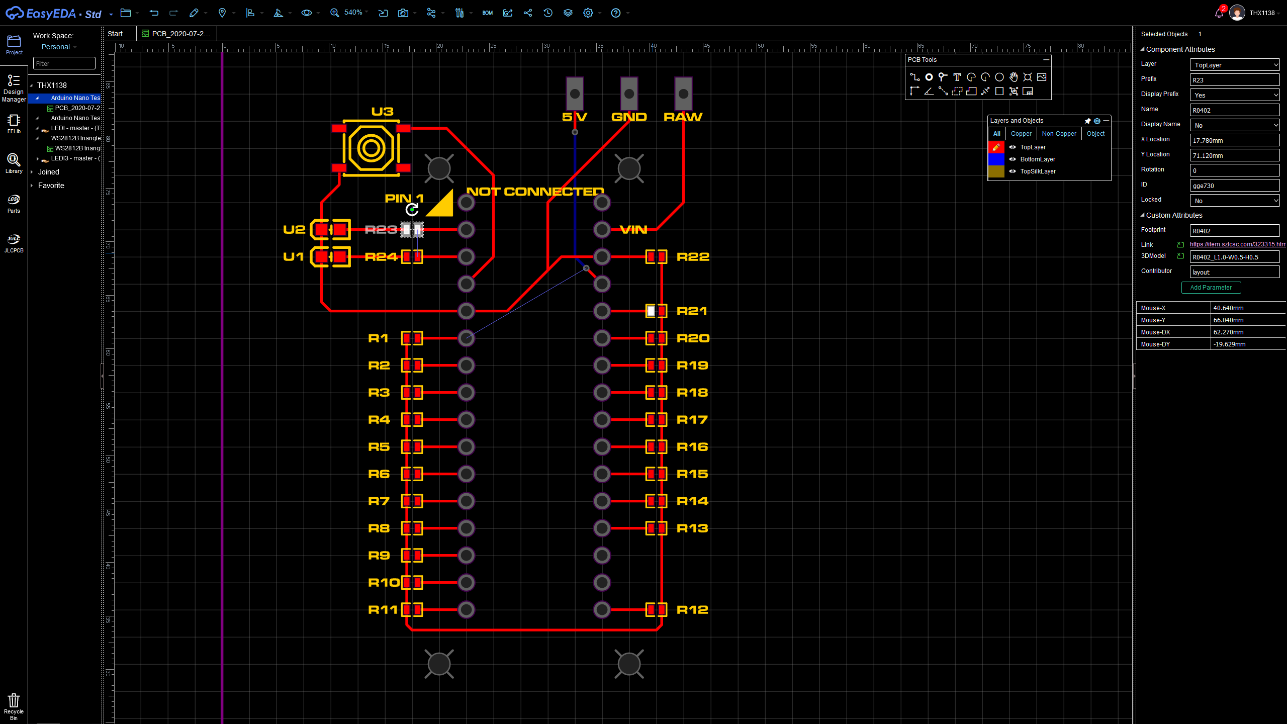
Hi. I'm new to EasyEDA and wanted to make what I think is a fairly simple PCB so I didn't make a schematic first. I used the library to add parts but it seems like EasyEDA is not remembering the exact parts I added and is only remembering the footprint. I wanted to use the SMT assembly service so the software obviously needs to know exactly what parts I need. The link in the right hand panel is the same for all the resistors and when I export a BOM, it says there is only one value of resistor when there are actually meant to be four values. Is it not possible to use the SMT assembly service without making a schematic first? ![delme.png](//image.easyeda.com/pullimage/ruAsyf8ozyCyf0KqOx1H5YIk9EKMbHCMfEEoymQm.png)
Comments
andyfierman 4 years ago
This is one of the reasons why we recommend always creating a complete schematic before doing Convert to PCB. By saving the time it takes to create that schematic you have now created a more time consuming task of having to manually edit your PCB-generated BoM. Fortunately your design is very simple so it may not take too long to identify the exact parts from the JLCPCB Assembled library that you have placed into your PCB and then manually fill in the missing information from the BoM and add the extra lines for the different valued parts. However, even with a simple design like this, the easiest and the safest way to fix this is to: 1. to make sure you do not change the PCB layout that you have at the moment, clone or make a backup of the project as it is now;  2. then, working on only the copy or the original project;  3. create a schematic with exactly the same reference designators (a.k.a. prefixes) as your PCB and;  4. add net labels with exactly the same names as have been auto-assigned in your PCB and;  5. use exactly the same components as you have used in your PCB and which therefore have the same PCB Footprints assigned to them then;  6. check that all the Schematic Symbol pin to PCB Footprint pad mappings are correct;  7. save it to the same project as your PCB;  8. run the Schematic Design Manager to check that your schematic is correct;  9. use the SHIFT+X Cross Probe tool to help you check that your PCB is the same as your Schematic. 10. generate your BoM from that schematic;  11. do **Update PCB...** from the Schematic Editor or **Import Changes...** in the PCB Editor;  12. the resulting PCB should be the same as before the update;  13. run the PCB Design Manager to check that your board is correct and there are no DRC errors. 14. generate the Gerbers;  15. download the Gerbers; 16. check the Gerbers using gerbv as advised in the Tutorial;  17. read the advisory notes on the order pages before you submit your PCB for manufacture and assembly; 18. before starting your next project in EasyEDA read all of the forum topic marked as [Must read], including the linked documents: [https://easyeda.com/forum/topic/How-to-ask-for-help-and-get-an-answer-71b17a40d15442349eaecbfae083e46a](https://easyeda.com/forum/topic/How-to-ask-for-help-and-get-an-answer-71b17a40d15442349eaecbfae083e46a)
Reply
Login or Register to add a comment
goToTop
你现在访问的是EasyEDA海外版,建议访问速度更快的国内版 https://lceda.cn(需要重新注册)
如果需要转移工程请在个人中心 - 工程 - 工程高级设置 - 下载工程,下载后在https://lceda.cn/editor 打开保存即可。
有问题联系QQ 3001956291 不再提醒
svg-battery svg-battery-wifi svg-books svg-more svg-paste svg-pencil svg-plant svg-ruler svg-share svg-user svg-logo-cn svg-double-arrow -mockplus- -mockplus- -mockplus- -mockplus- -mockplus- -mockplus- -mockplus- -mockplus-@1x -mockplus-

Cookie Notice

Our website uses essential cookies to help us ensure that it is working as expected, and uses optional analytics cookies to offer you a better browsing experience. To find out more, read our Cookie Notice