You need to use EasyEDA editor to create some projects before publishing
Making a faceplate - exposed copper issue
581 2
Tone Electronix 2 years ago
Hello! So I am trying to do a faceplate using text and graphics, exposing copper in a PCB, and I have some issues (and lack of knowledge). I found this topic ([https://easyeda.com/forum/topic/expose-coper-of-text-object-8a343e5137464bf997da75568d7ff2e7](https://easyeda.com/forum/topic/expose-coper-of-text-object-8a343e5137464bf997da75568d7ff2e7)) and this is what I did: 
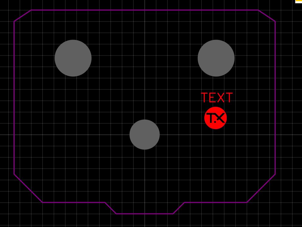
1- the faceplate is this, three holes for potentiometers (grey ones) and outlines in purple. The text and symbol I am testing: ![Capturar1.JPG](//image.easyeda.com/pullimage/52QpJ6DL22J1cLyub7wtWm7hql7xftoIBh0GUTRW.jpeg) 
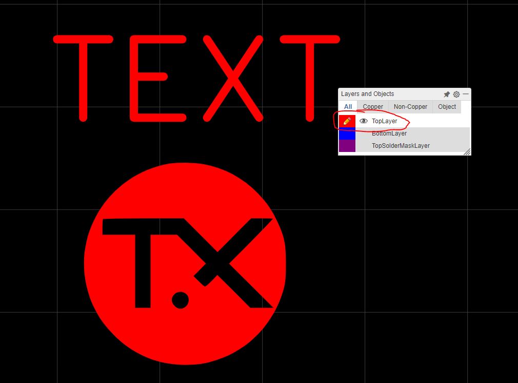
2- so I added 2x copies of each text AND graphic. One of each to "Top Layer": ![Capturar2.JPG](//image.easyeda.com/pullimage/BLtC1g9WLn7lom9l2jDYQJMNfGoYyOVLsMAGofgZ.jpeg) 
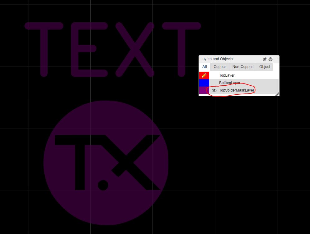
3- and the other on "Top Solder Mask Layer": ![Capturar3.JPG](//image.easyeda.com/pullimage/jzk9YRq7YoWX3laGv9YkXPZMTo8XIajAF3jB0ktp.jpeg) <br> Now the question is, what do I do next?? Mind that this is not a "electronic schematic", it's just a design. Should I add a "net" (GND for example)???? Thank you for your help!
Comments
andyfierman 2 years ago
Pads are automatically exposed copper. You could also try: Create your text then export it as DXF; Import > DXF into the Top Layer; Select, right-click > Convert to Board Cutout; Then Select the Board Cutout (not the vertices); In the upper right hand panel, select Solid (should default to Top Layer); Then Select the Solid Region (not the vertices); Right-click > Convert to Pad.
Reply
andyfierman 2 years ago
Once the elements are instantiated as pads, they can all be assigned a pad number and a net name The pad number and net name can be the same for all of the created pad elements or they can be different for each element. Ignore any ratlines and the PCB Design Manager warnings.
Reply
Login or Register to add a comment
goToTop
你现在访问的是EasyEDA海外版,使用建立访问速度更快的国内版 https://lceda.cn(需要重新注册)
如果需要转移工程请在个人中心 - 工程 - 工程高级设置 - 下载工程,下载后在https://lceda.cn/editor 打开保存即可。
有问题联系QQ 3001956291 不再提醒
svg-battery svg-battery-wifi svg-books svg-more svg-paste svg-pencil svg-plant svg-ruler svg-share svg-user svg-logo-cn svg-double-arrow -mockplus- -mockplus- -mockplus- -mockplus- -mockplus- -mockplus- -mockplus- -mockplus-@1x -mockplus-

Cookie Notice

Our website uses essential cookies to help us ensure that it is working as expected, and uses optional analytics cookies to offer you a better browsing experience. To find out more, read our Cookie Notice