Hello -
Is it normal for the system to assign multiple net names to vias or pads connected together? Shouldn't they all be the same net (0)?
Thank you,

Not sure if I've already pointed you to this howto but it might help:
[https://easyeda.com/forum/topic/How-to-place-multiple-vias-in-a-PCB-footprint-a34cf68d58414138898a56de60abd8c1](https://easyeda.com/forum/topic/How-to-place-multiple-vias-in-a-PCB-footprint-a34cf68d58414138898a56de60abd8c1)
If your PCB is drawn directly in the PCB editor then you need to see:
[https://easyeda\.com/forum/topic/How\_does\_the\_Connect\_Pad\_to\_Pad\_tool\_work\_\-JgQO0Ay7H](https://easyeda.com/forum/topic/How_does_the_Connect_Pad_to_Pad_tool_work_-JgQO0Ay7H)
Can you please open my board and see the problem, copper area not connecting to through hole pads with same net name. On top layer only. Works on all other layers...
I looked for your board on your page last night but did not see anything that had a structure that looked like your screenshot.
Can you post the URL to a public copy?
In the PCB lib
OK, from your post:
[https://easyeda.com/forum/topic/Copper-Area-Not-Connection-To-Thermal-Vias-572f38ac04b7471dba2a0d8db6537bb4](https://easyeda.com/forum/topic/Copper-Area-Not-Connection-To-Thermal-Vias-572f38ac04b7471dba2a0d8db6537bb4)
here's your PCB Lib:
[https://easyeda\.com/editor\#id=0f9d083a4b19494ea097b60770f5fa70\|505cde11d9b74e6696e02b822c4c344c\|\!46a2d48d2ead4cf5bdd98bf1eda9ebd4\|\!3d7bfd5fd4944df58b100427444799ca](https://easyeda.com/editor#id=0f9d083a4b19494ea097b60770f5fa70|505cde11d9b74e6696e02b822c4c344c|!46a2d48d2ead4cf5bdd98bf1eda9ebd4|!3d7bfd5fd4944df58b100427444799ca)
I think what you could do is to is to remove the tracking and recreate the connections to all the vias by forming a suitably shaped polygon pad, in a similar way that you have tried to do with a Solid Region here:
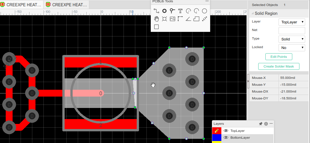
Assign the pin number of the polygon pads to be the same as that of the vias and the centre pad.
As you have already done, leave the Net attributes blank.
Another possibility might be to use small rectangular pads to link all the vias to the centre pad in a piecewise fashion and again, assign them the same pin number as the vias and the centre pad with the Net attributes left blank.
Our website uses essential cookies to help us ensure that it is working as expected, and uses optional analytics cookies to offer you a better browsing experience. To find out more, read our Cookie Notice


 Brand new interactions and interfaces.


 Easy to use and quick to get started.