
<span class="colour" style="color: rgb(215, 218, 220);">Hi!</span>
<span class="colour" style="color: rgb(215, 218, 220);">i'm trying to build a THT version of the onboard preamp Aguilar OBP-3. I'm new using Easy Eda and i cannot figure how to solve this netlabel problem for V+ and GND. I've also done a smd version and it doesn't have this issue, all i have done is replacing the parts one by one and i used pads instead of connectors (since this is quite bigger i wanted to save space). Here it is the project with the schematics: [Aguilar OBP-3 THT](https://oshwlab.com/difesa98/aguilar-obp-3-pth)</span>
<span class="colour" style="color: rgb(215, 218, 220);">I used the autorouter for this project, is it reliable? for a 45x50 mm board it used 1700 mm of copper, maybe it could be a problem in term of noise? When everything will be ok, how could i obtain the frequency response of this preamp? Here it is a diagram made by Ibanez for the original one.</span>
<span class="colour" style="color: rgb(215, 218, 220);"> 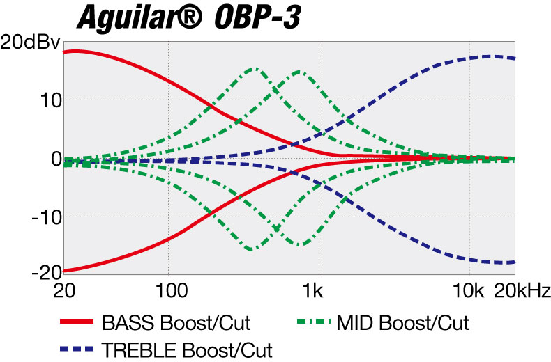</span>
<span class="colour" style="color: rgb(215, 218, 220);">Thank you for any advice!</span>


 Brand new interactions and interfaces.


 Easy to use and quick to get started.