Hi
Can you send your PCB to [support@easyeda.com](mailto:support@easyeda.com)?
we will check it.
[https://docs.easyeda.com/en/Export/Export-EasyEDA-Source-File/index.html](https://docs.easyeda.com/en/Export/Export-EasyEDA-Source-File/index.html)
Sent you a copy. Also since then I've found the ground plane is connected to components it shouldn't be - and DRC doesn't catch it. See D6 cathode and the track next to it. Left no ground plane, right with ground plane ! Can we go back to the previous release until this release is properly tested please ?
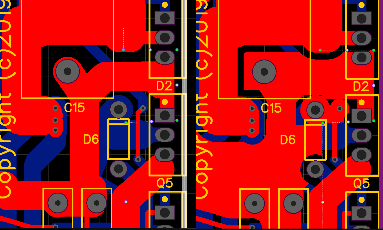
And it seems Keep Island -> No has stopped working as well (bit in top left)
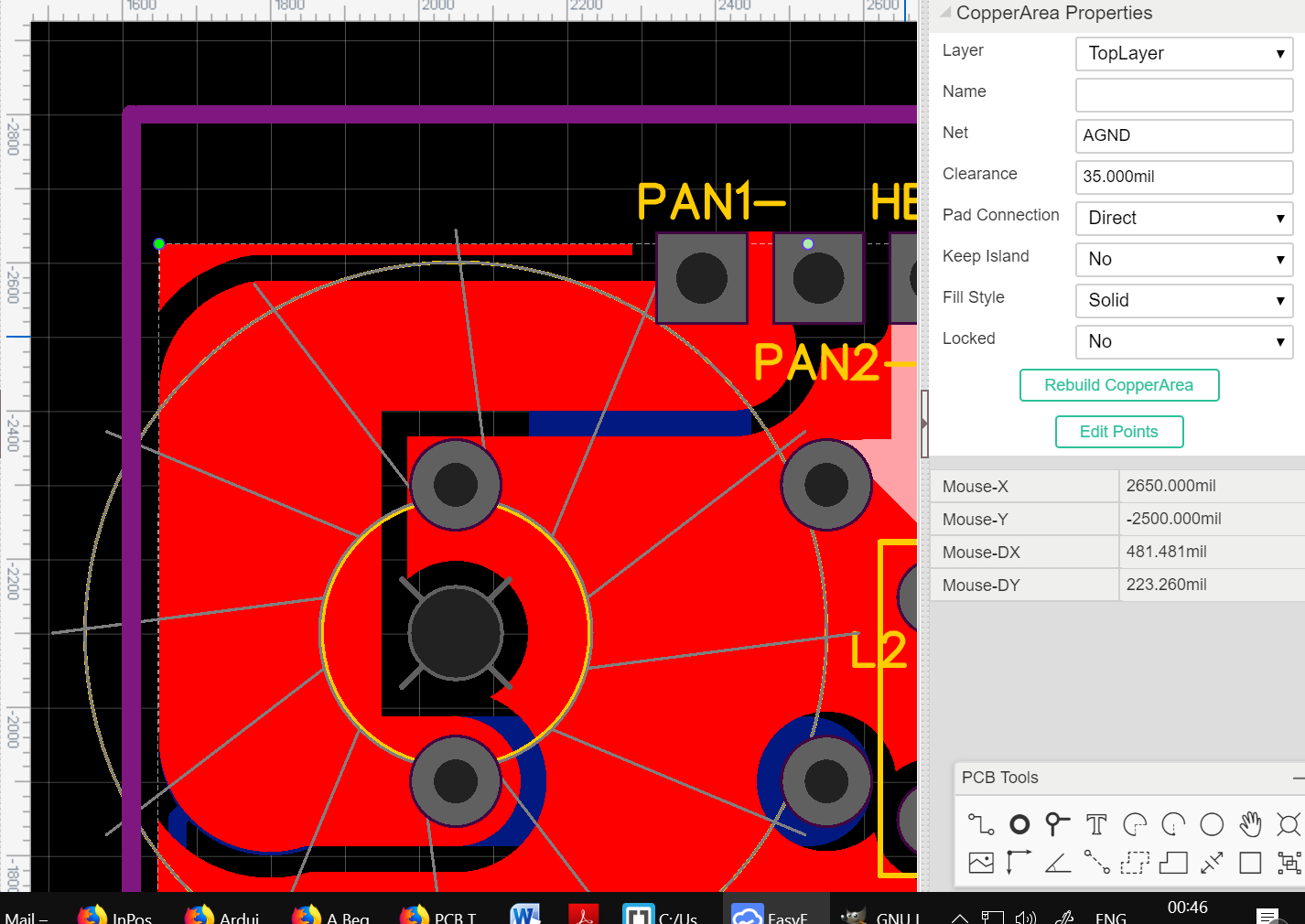
Just testing it now. One small problem that isn't important is it doesn't always rebuild correctly when you press Rebuild Copper Area, but does do it correctly if you move any of the outline nodes to a different position then back again.
Here's one of many - and this one is always wrong. The plane above R8. Others tend to be more random.
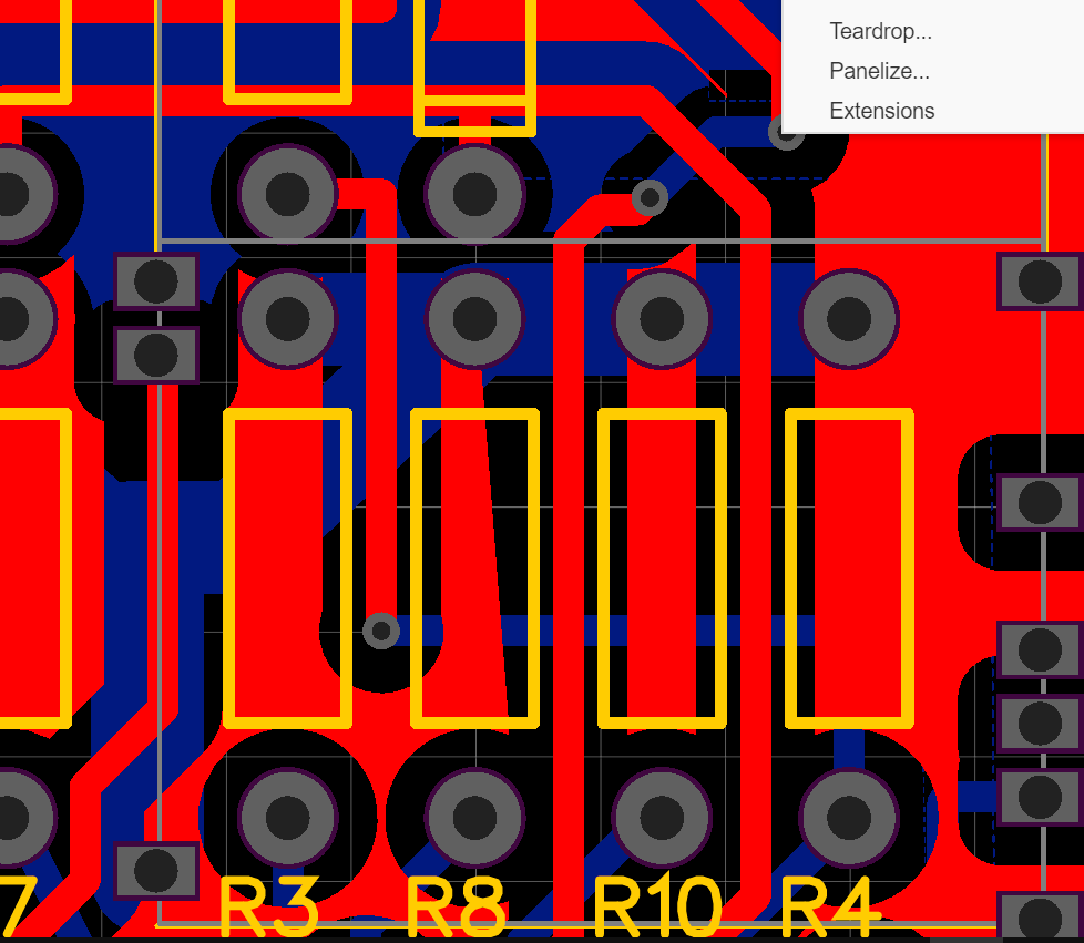
Can you try to disable the hardware acceleration?
After we testing, this option will impact the copper pour.

I'm running Chrome in the packaged version that comes with EasyEDA. Chrome isn't on my Windows menu as a standalone app. How do I get to the Hardware acceleration screen you show ?
@MikeDB
You can find at the "Settings"
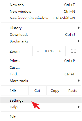
if you turn off the Hardware acceleration option the copper area works well, that should be the browser's bug, it is only impact the vision, the gerber still correct.
@UserSupport
I use the version of Chrome that downloads with EasyEDA so I never see that menu as it starts up in full screen. I've tried F11 and all the normal tricks but it never appears.
@UserSupport
Yes all seems to be working perfectly now. Once again many thanks for your swift fix - it really is appreciated how quickly you fix problems on what is a free to use tool. I used to wait months for fixes on CadStar and I expect you know how much that costs !
Keep up the **exceptional** work and a Happy New Year !!
@UserSupport
How many people do you have working on EasyEDA development ? I'm new to this tool so not sure of the setup other than the link with JLC and LCSC who I've used on the two boards ordered so far.
Hi, after the new release this morning, when adding new TRACK the area that surrounds the copper is not updated, it is not cleared, the only way to clear it is to run auto router. Yesterday this worked fine.
Filipe
Here is an example, teh white line is the TRACK and you can see that it does not update with the clearance spacing.
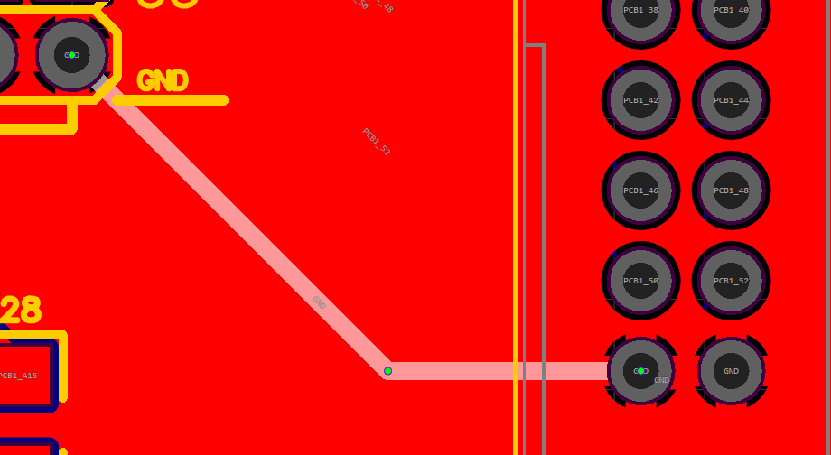
that was a bad example as it was GND, here is another one, I deleted the TRACK PCB1_A15 and it does not update with copper
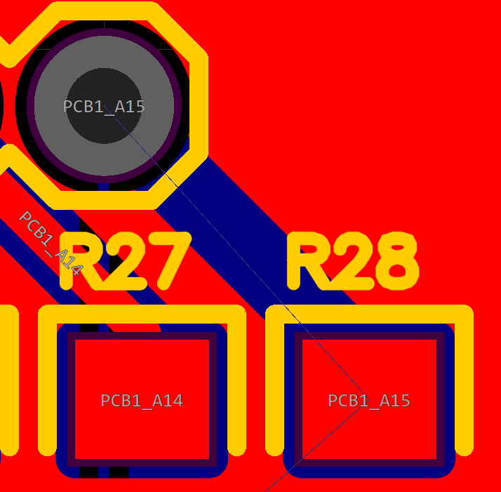
@ct1ilt
when the track and copper are the same net, they won't generate the clearance. when you draw a different net track, you need to shift+b to rebuild the copper area.
it used to work without doing shift-b and since this morning after update it does not work anymore, after every track I make I need to make shift-b, this is painful
Our website uses essential cookies to help us ensure that it is working as expected, and uses optional analytics cookies to offer you a better browsing experience. To find out more, read our Cookie Notice