
Hello,
I have designed a component (which is a antenna bluetooth printed in the board) to be placed in the board.
I want to do it in the same way of the next picture:
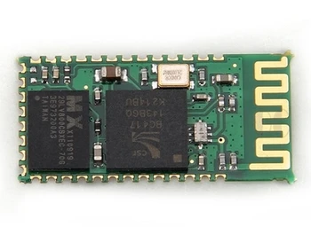
That is, cooper area, but the gerber can't say this area will have tin (lead free). I mean, I wan't the stencil to have this are routed.
How can I keep a copper area visible, and avoid this mark in the stencil?
Thanks in advance


 Brand new interactions and interfaces.


 Easy to use and quick to get started.