You need to use EasyEDA editor to create some projects before publishing
PCB Track Current Capacity
1884 27
JulesP 3 years ago
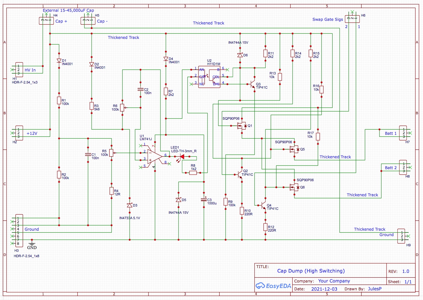
I have a query regarding the solder tracks on a PCB that I have designed (attached). Due to high pulse currents from a capacitor, of the order of 50-120A, some of the tracks on the PCB will need to be enhanced by, if possible, adding solder to a regular track of say 4-5mm width. I don’t know what the current carrying capacity of such tracks is so maybe you have some data on this for different track dimensions of standard thickness? Besides that, do you also know if the protective resin layer on the top of a PCB will melt away with the heat of a soldering iron so I can add extra solder, or if it will resist such heat and prevent me from thickening the track? Thanks, Jules ![Cap Dump Schematic.jpeg](//image.easyeda.com/pullimage/P006SApUaO3N6Mttn7Bhrra1L1pd65KlNCIpsnrt.jpeg)
Comments
andyfierman 3 years ago
You can select the relevant segments of track and then click **Expose Copper**: ![image.png](//image.easyeda.com/pullimage/01mhw79sOBBmeMbTA2OgGoowImLHWHZfQLlOpGPR.png) This will remove the solder resist over the segment leaving it open for additional solder to be applied.
Reply
JulesP 3 years ago
Thanks Andy. Do you have any data on how much current a track of a specific width can take without overheating? Pulses will average out the heat over time but I could make a guestimate if there is any published data.
Reply
JulesP 3 years ago
. . . or if I knew the thickness I could calculate the resistivity and go from there.
Reply
andyfierman 3 years ago
A couple of points about your schematic. 1. You should not draw or extend wires so that they overlap the ends of symbol pins: you do not need to show a join dot where a single wire joins a pin;  2. The left hand side of the schematic is reasonably clear and tidy. The right hand side is cluttered and almost unreadable. A tidy schematic is much easier for everyone to read and significantly helps in avoiding connectivity mistakes; 3. If I read your circuit correctly, you are using U2 to turn on Q3 and so pull the gate of Q1 down towards ground hence turning Q1 on. The problem is that R9 is shown as 100k. Did you intend it to be 220R as in R10 and R12? 4. When you turn off U2, there is nothing actively pulling charge back out of Q3 base emitter junction so Q3 will be very slow to turn off and may be prone to turning on with noise spikes or RFI;  5. If you are going to use an opto-isolator then you should make the supplies and ground of the 741 control circuit completely separate from the noisy high current tracks. As you have drawn it, the ground for the 741 appears to share the ground return from the cap discharge current; 6. If you are going to the trouble of heavily decoupling the positive supply to the 741 with the diode and 1000uF cap then why do you need an opto-coupler when with careful routing you could design a simple gate drive without one? 7. There are better choices for a comparator than a 741 op amp. It does work as a comparator (even though not designed to) but has very little useful output swing even when run off 12V and is dog slow. A comparator with an open collector output such as an LM319 or push-pull output device such as the TLV3501 would probably be a better choice and simplify driving either the opto-isolator or the MOSFET more directly. You may find it helpful to read: [https://easyeda.com/forum/topic/How-to-ask-for-help-and-get-an-answer-71b17a40d15442349eaecbfae083e46a](https://easyeda.com/forum/topic/How-to-ask-for-help-and-get-an-answer-71b17a40d15442349eaecbfae083e46a)<br> <br> In particular, (2.2), (4) and (6) in (2) in the above will help avoid a lot of hassle. Here are some simulation examples of comparators. [https://easyeda\.com/example/The\_EasyEDA\_LM319\_spice\_models\-MA6oGAR9r](https://easyeda.com/example/The_EasyEDA_LM319_spice_models-MA6oGAR9r) [https://easyeda\.com/andyfierman/Inverting\_comparator\_with\_hysteresis\-87a982dc29b24c1cb835e939a0659d70](https://easyeda.com/andyfierman/Inverting_comparator_with_hysteresis-87a982dc29b24c1cb835e939a0659d70) [https://easyeda.com/andyfierman/TLV3501_comparator-6EM3XfxrJ](https://easyeda.com/andyfierman/TLV3501_comparator-6EM3XfxrJ)<br> <br>
Reply
andyfierman 3 years ago
Ooops, Sorry: just realised who you are after you changed your avatar. So you probably already know where the stuff I linked to is. Temperature vs. current vs. track width: [https://easyeda.com/forum/topic/Copper-Trail-fot-mains-240-V-supply-6159cdb343ee4cc48d50bcf53a21c19d](https://easyeda.com/forum/topic/Copper-Trail-fot-mains-240-V-supply-6159cdb343ee4cc48d50bcf53a21c19d) [https://easyeda.com/forum/topic/PCB-high-current-thermal-design-562f7a69a7ad41a38b18ea150d6703ed](https://easyeda.com/forum/topic/PCB-high-current-thermal-design-562f7a69a7ad41a38b18ea150d6703ed)<br> <br> See also PCB Tools in: [https://easyeda.com/forum/topic/Extension-User-Extensions-for-EasyEDA-Summary-9e065b68316f4491a3911dc6204be31e](https://easyeda.com/forum/topic/Extension-User-Extensions-for-EasyEDA-Summary-9e065b68316f4491a3911dc6204be31e)
Reply
JulesP 3 years ago
Andy, I appreciate your comments on the circuit. It was developed from a low sided one doing the same job. Re: 1:  Having had connection issues before I was making doubly certain. 2: Yes it needs some tidying. 3: Yes it should be 220R, not 100k (imported resistor from another of my schematics and forgot to change it). 4: Would a 1k resistor to Ground help with that? 5: I can run the op-amp from a separate 12V supply and ground easily enough, connected from the mainboard. 6: Don't know. That was the original design that has worked with others.  I  understand it will still work even if the isolation is 'overkill'. 7: I will look into using an LM319. I assume your links above will suggest a suitable configuration to achieve the same function? Regarding thermal issues, a thin wide PCB track will dissipate heat differently to a round wire core of the same resistance and I was looking for clarity on that. Will survey the forum for info. J <br> <br>
Reply
JulesP 3 years ago
Here is a revised schematic: ![Cap Dump Schematic.jpeg](//image.easyeda.com/pullimage/WcOk4Tc4Vm82SKVaLwDx45mrUm5D8NIVhJrCMcaf.jpeg)
Reply
andyfierman 3 years ago
"Would a 1k resistor to Ground help with that?" Not sure. Maybe there's a reason to do it like that but the whole way the output of U2 and Q3 are connected to pull the gate of Q1 down is weird. I'd recommend redesigning it into a more standard - and more easily understandable - form of gate drive. Some simulation work in EasyEDA would speed up and improve confidence in the design. * I have just realised that the symbols that you have specified SQP90P06 P channel MOSFETs but the symbols you have placed are for N channel MOSFETs! Check the SQP90P06 datasheet: [https://www.farnell.com/datasheets/3006549.pdf](https://www.farnell.com/datasheets/3006549.pdf)<br> <br> <br> "I can run the op-amp from a separate 12V supply and ground easily enough, connected from the mainboard." You need to do that with anything associated with the input side of the 741 so the pot circuitry needs to be included in that. <br> "I will look into using an LM319. I assume your links above will suggest a suitable configuration to achieve the same function?" They are simulations showing fairly generic usage cases and not specifically for driving the input to an optocoupler. I don't understand what the two pots are for on the inputs to the 741 and so exactly what the output is expected to do but I was assuming that it is required to change state quickly to turn the LED in the optocoupler on and off rather than do something in a linear fashion. If it's used as a comparator then replacing it with an LM319 and simply connecting the open collector output to the cathode of the LED in the opto coupler through a suitable resistor is all that is required. You do have to pay careful attention to the LM319 datasheet and in particular how the input currents of the LM319 change with the voltage difference between them as it behaves differently from an op amp and so may produce slightly puzzling voltages if you measure them at the pot sliders. Adding resistors in series between the pot sliders and the LM319 inputs should alleviate that issue. It may be helpful to add a small amount of hysteresis to give clean switching points with no "fizzing" which could damage the MOSFETs by them not cleanly switching from off to on. The resistor value is approximately \(VP\-Vf\_LED\-Vsat\_319\)/I\_LED where VP is the supply voltage; Vf_LED is the typical forward voltage of the LED in the opto; Vsat_319 is the typical saturation voltage across the output transistor in its on state; I_LED is the desired curren through the LED. <br> So for a 12V supply, a typical LED voltage is 1V and the saturation voltage of the LM319 of 0.5V if you want 10mA through the opto LED then the series resistor is 10.5V/10mA = approx 1K. <br> "Regarding thermal issues, a thin wide PCB track will dissipate heat differently to a round wire core of the same resistance and I was looking for clarity on that." I understood from your question that you wanted to work out PCB track widths vs. current and temperature rise so the calculators I suggested in the links (I haven't used the one that in the Extensions Topic) are all specifically for PCB traces and not wires in free air or with insulated coatings.
Reply
JulesP 3 years ago
> I'd recommend redesigning it into a more standard - and more easily understandable - form of gate drive. Some simulation work in EasyEDA would speed up and improve confidence in the design. I don't trust my confidence to use the simulation effectively to improve the design but I may have a go at some point. I'm relying on the fact that this method and the circuit has worked for others over at least a decade. It may not be the optimum design and mine is just a high sided switched version due to the topology of the rest of my already built circuit and for which I am currently replacing the Veroboard setup with a PCB. This cap dump circuit is for the next phase. > I have just realised that the symbols that you have specified SQP90P06 P channel MOSFETs but the symbols you have placed are for N channel MOSFETs! Check the SQP90P06 datasheet: Another case of my importing a TO-220 footprint for positioning and not going to the library. Done now. > You need to do that with anything associated with the input side of the 741 so the pot circuitry needs to be included in that. Modified. > I don't understand what the two pots are for on the inputs to the 741 and so exactly what the output is expected to do As I understand it R5 sets the voltage at which the cap starts to discharge and is optimally set to 24V. R6 sets the hysteresis and the point at which discharge to the battery stops, normally 17V. So yes the optocoupler will be required to quickly and promptly shut off. > Adding resistors in series between the pot sliders and the LM319 inputs should alleviate that issue. I've inserted two 500R ones but that was just a guess. > It may be helpful to add a small amount of hysteresis to give clean switching points with no "fizzing" which could damage the MOSFETs by them not cleanly switching from off to on. Is this a revised value for R8 (1k2)? (R10 in the latest schematic) > calculators I suggested in the links (I haven't used the one that in the Extensions Topic) are all specifically for PCB traces and not wires in free air or with insulated coatings. Sure but as I'm going to need to add solder to a bare track, the conduit will be more like a wire. So the tables won't be applicable here and I'm just going to have to guess. If the current is too much for the circuit I can reduce the storage cap from 45,000uF to 15,000uF which will reduce the charge being released, and hence current, but do it more frequently. ![Cap Dump Schematic.jpeg](//image.easyeda.com/pullimage/7eumbwNTJPb1zsvMcBps6WXIUHu5s7H388lIUW7T.jpeg)
Reply
JulesP 3 years ago
> I don't understand what the two pots are for on the inputs to the 741 and so exactly what the output is expected to do As I understand it R5 sets the voltage at which the cap starts to discharge and is optimally set to 24V. R6 sets the hysteresis and the point at which discharge to the battery stops, normally 17V. So yes the optocoupler will be required to quickly and promptly shut off. These two statements got merged.
Reply
andyfierman 3 years ago
The conductivity of solder is a lot lower than that of copper so your first approach might be to use the PCB track calculator but allow a higher track temperature than for the final thickened track, design for that copper (probably pay the extra and get a 2oz copper board) and then assume that you are going to put say an extra 1mm thick layer of solder on top of the copper. So that gives you a rectangular cross section of copper of the track thickness high by the track width, in parallel with a rectangular cross section of copper 1mm high by the width of the track. They're simple geometries for which to work out the resistance of each per unit length at room temperature. For a first approximation (and probably an adequate estimate) you don't need to worry abut the actual temperature at this stage, just assume that the resistivity of both copper and solder is proportional to absolute temperature. Then you know that at room temperature when you put the two in parallel the total resistance of the copper track will be reduced by that of the added solder. Therefore the power dissipation at a given current will drop by the reduction in resistance. Hence a reasonable estimate is that the temperature will drop by the same ratio. Say adding the solder reduces the resistance from R to R*2/3 so the power dissipation at a current I drops by 2/3 so the temperature drops by 2/3. I don't know the resistivity of solder compared to copper but you'll be able to find that out easily enough from the web.
Reply
andyfierman 3 years ago
Sorry: I forgot that the LM319 is a dual comparator. The LM311 is similar but a single device. It's response time is 200ns instead of 80ns but that should still be fast enough. With either of them you must ground the GND pin. You cannot leave it unconnected as you have shown in the schematic..
Reply
andyfierman 3 years ago
I hadn't spotted that there is already hysteresis around the 741.
Reply
JulesP 3 years ago
Andy, Thanks for the track info and suggestions. Here is the updated sheet with the LM311. Pin 4 of that is for Vee but I doubt that's relevant. I have also removed the 15V Zener (was D5 in the earlier schematic) as I don't think that will serve much purpose with the dedicated 12V supply. Are R7 & R8 at 500R ok? I have also set R10 to 1k. Thanks <br> ![Cap Dump Schematic.jpeg](//image.easyeda.com/pullimage/QUCS9t2Ku4jd4on45dCLuG6LFshxxQ838NoRMZyJ.jpeg)
Reply
andyfierman 3 years ago
@JulesP, "Here is the updated sheet with the LM311. Pin 4 of that is for Vee but I doubt that's relevant." Sorry but you need to study the datasheet for the LM311 carefully and make sure that you understand what the pins on this device are all for: [https://www.ti.com/lit/ds/symlink/lm311.pdf](https://www.ti.com/lit/ds/symlink/lm311.pdf)<br> <br> Figs 9 and 22 shows application examples similar to yours. In your application, both pin 1 **and** pin 4 must go to ground. If you're not sure how to adapt the design to use a comparator like this with a floating output switch output instead of a push-pull output like the 741 then you are probably better off either reverting to the original 741 based comparator or sourcing a suitable push-pull output comparator such as: LMC7211 TLV7211 [https://www.ti.com/product/LMC7211-N](https://www.ti.com/product/LMC7211-N) [https://www.ti.com/lit/gpn/TLV7211](https://www.ti.com/lit/gpn/TLV7211)<br> <br> Overall it looks like the circuit is doing a relatively simple task so with a good, clear Design Requirements Specification (DRS), I think there is a lot of stuff that could be simplified so the schematic and PCB design could be a lot simpler than your current schematic suggests. So, another option is that I could redesign it including the PCB for you but that would need a more detailed DRS which may be beyond the budget for this project. * Note that, instead of just writing "Thickened track", you can selectively change the wire thickness in the right hand panel. That would make it much easier to identify them. Like this: [https://easyeda\.com/example/Automotive\_12V\_to\_USB\_5V\_2A\_output\_power\_adapter\_\-L1xrlfxrJ](https://easyeda.com/example/Automotive_12V_to_USB_5V_2A_output_power_adapter_-L1xrlfxrJ)
Reply
JulesP 3 years ago
Thanks, I'll set my extra homework :)
Reply
JulesP 3 years ago
I've gone for a simpler dual package comparator the TS372 with its push-pull output. It seems the floating ones will need more circuitry. ![Cap Dump Schematic.jpeg](//image.easyeda.com/pullimage/l7cIuLofY8fCtaZcdhaQvSIyPA2FZEIcQxq2hnfz.jpeg)
Reply
andyfierman 3 years ago
@JulesP, But the TS372 is not  push-pull: it's an open drain output... [https://www.st.com/resource/en/datasheet/ts372.pdf](https://www.st.com/resource/en/datasheet/ts372.pdf)<br> <br> Did you mean the TS3702 and TSX3702? [https://www.st.com/en/amplifiers-and-comparators/ts3702.html](https://www.st.com/en/amplifiers-and-comparators/ts3702.html) [https://www.st.com/en/amplifiers-and-comparators/tsx3702.html](https://www.st.com/en/amplifiers-and-comparators/tsx3702.html)<br> <br> Also, you've accidentally removed the hysteresis connection from the output of the comparator and connected it to the positive supply of the comparator: ![image.png](//image.easyeda.com/pullimage/UwGbsPDhMoJkH86w8PQj0H1qtqcixABYxQa6JqIP.png)
Reply
JulesP 3 years ago
Yes on both counts :) Thank you kindly for your help.
Reply
JulesP 3 years ago
Voila! ![Cap Dump Schematic.jpeg](//image.easyeda.com/pullimage/nu02l3SC3QTcVAgVdLJGcPUYVYeOzePtzxE31jg8.jpeg)
Reply
JulesP 2 years ago
Hi Andy, I have prepared my PCB for the Cap Dump circuit, that you kindly reviewed (see attached), but just before I was going to send it for production I started to get a niggling feeling about the setup (biasing) of the two TIP41C BJTs (Q2&4) that trigger the P channel FETs (Q5&6) when their Collectors go Low, and whether they would cope with the resulting voltages. To check this out I drew up the relevant part of the circuit and could not get the calculated voltages, like VRC, to be anything sensible. So I have come up with an alternative using N-Channel FETs instead. I show these two options side by side in the attached pic. My query is, will the BJT option not work well or at all and the FET option be preferable and, if so, do I need to tweak the values of R15 and R17? The full current schematic is in the previous post. Thanks Jules ![Cap Dump V1 PCB 3.jpeg](//image.easyeda.com/pullimage/moKBdde7rG8clUz67O1ujCaEY8PuMOmEvCh84w6S.jpeg) ![BJT vs FET for Cap Dump Logic.jpeg](//image.easyeda.com/pullimage/6K3Ab7Q1Ju8Sc47XUqip23vTcDPctoW34yTWzDY1.jpeg) <br> <br>
Reply
andyfierman 2 years ago
"To check this out I drew up the relevant part of the circuit and could not get the calculated voltages, like VRC, to be anything sensible." Sorry but I looking on my phone, I can't spot VRC and I don't know how or under what conditions you worked out that voltage. There are so many off-board parts to your circuit that I can't see how it is intended to work or how and to what everything is connected. The best way to verify this is to build a simulation of the relevant parts of the schematic. This should include the connections to Q6 to see dynamic performance. Include the load circuitry if you want to see the power dissipation in Q6 and any other devices in the pulsed high current path. What voltage do you require at the gate of Q6 with Q4 on and with Q4 off? What rise and fall times do you require? What does the connection labelled as 12V do when Q4 is being turned on and off
Reply
andyfierman 2 years ago
If your bjt version is really supplied from 12V through a 10R source resistance then, no, it will not do what you require and the mosfet version may be better suited but without a schematic that shows all those off board connections that include other connections to the base of Q4 it is not clear exactly how the base of Q4 is really driven. As shown in your snippet\, the emitter of Q4 will pull up to \(12V \- Q4\_Vbe \- Q4\_Ib\*10\) so the gate drive to Q6 can only pull down to that voltage plus Q4\_Vcesat\. As you have drawn it, the mosfet version will pull the gate drive to Q6 down to ground.
Reply
andyfierman 2 years ago
I have to pint out that your PCB layout is a disaster waiting to happen. You have routed the high side highcurrent path round the upper right of the board and the low side return current path round the lower left. This makes a loop enclosing much of the other circuitry. Do when you discharge the cap, a big magnetic field pulse is generated which may induce unexpected currents not just in your circuit but in other external stuff. This may cause unexpected behaviour and may cause damage. You should at the very least route the high current paths as short and as close as possible parallel to each other to absolutely minimise the loop are that the total path encloses, with nothing inside that loop. I'm not fishing for work here but if you need help with this project, I can be hired to sort out the schematic the pcb layout. However I suspect your budget may not stretch to that. :)
Reply
JulesP 2 years ago
Hi Andy, Vrc is not showing but it was one of the voltages I tried to calculate based on the BJT version to see if it made sense. In the BJT version the base of Q4 is just driven as shown, by a branch from the Gate feeds of the two 'Swap FETs'. In the MOSFET version, I need the Gate of Q6 (P-channel device) to be pulled down so that it will switch on. I was wondering if the resistors R15&17 were appropriate. So you can see the 'off board' connections here is the main PCB schematic. As you can see the Swap Gate 1&2 on the Cap Dump Circuit come from the Gates of the Swap FETs Q2 and Q3. I also attach the Truth table for how the Cap Dump circuit should direct the pulses to the right battery and the modified schematic showing the FET option for the Cap Dump circuit. I expect you are right that a mag field will be produced but I do have a copper area connected to Ground on both layers. Won't that help? The challenge I had with the routing of the Cap + line is that I had to avoid the outputs of the Drain of Q1 crossing over each other to Q5&6. I expect I can reroute the Cap- path over the top and to the left of the + line and behind the Q1 heat sink to avoid a loop. As you say it's much cheaper for me to have a go :) ![BEMF Generator Schematic V2.jpeg](//image.easyeda.com/pullimage/uP15xYKqZ36EWzke5jlRDZhlOOTkAXd3LEh8qM8M.jpeg) ![Cap Pulse Truth table.jpeg](//image.easyeda.com/pullimage/Y8ZG9j57LJnIgLeOlKuOKSanrHD4g50AXuRgNRvZ.jpeg) ![Cap Dump Schematic v1A.jpeg](//image.easyeda.com/pullimage/VJ6e9BMZiUB4XvRHr6r1XoA02ZuLbhpfRJlWGCnd.jpeg)
Reply
JulesP 2 years ago
Incidentally, the main PCB is already built and working fine. The Cap dump circuit is an extension to it.
Reply
JulesP 2 years ago
. . . and here is the revised PCB with the only components being in a current loop are 2/3 of the FETs with their ally heatsinks. I think they are robust enough to withstand some transient mag fields. ![Cap Dump V1 PCB 3.jpeg](//image.easyeda.com/pullimage/Fyzn5lcOMKVfE24diM7qYK7tTcnPhB5zUmMDmc1f.jpeg)
Reply
Login or Register to add a comment
goToTop
你现在访问的是EasyEDA海外版,建议访问速度更快的国内版 https://lceda.cn(需要重新注册)
如果需要转移工程请在个人中心 - 工程 - 工程高级设置 - 下载工程,下载后在https://lceda.cn/editor 打开保存即可。
有问题联系QQ 3001956291 不再提醒
svg-battery svg-battery-wifi svg-books svg-more svg-paste svg-pencil svg-plant svg-ruler svg-share svg-user svg-logo-cn svg-double-arrow -mockplus- -mockplus- -mockplus- -mockplus- -mockplus- -mockplus- -mockplus- -mockplus-@1x -mockplus-

Cookie Notice

Our website uses essential cookies to help us ensure that it is working as expected, and uses optional analytics cookies to offer you a better browsing experience. To find out more, read our Cookie Notice