
In my reply to this post:
[https://easyeda.com/forum/topic/One-schematic-two-PCB-ea8aef2c6cc54b80b525f30632ab0eb9](https://easyeda.com/forum/topic/One-schematic-two-PCB-ea8aef2c6cc54b80b525f30632ab0eb9)<br>
<br>
where the user wants to make one PCB which can be snapped into two and connected at right angles to each other like this:

I suggested that the OP simply draw a V-Cut line across the PCB in the Board Outline layer so that it could be snapped into two halves like in this example:

The OP did this but then they found that the <span class="colour" style="color: rgb(85, 85, 85);">2D model only showed one half of the PCB: </span><br>
<br>
<span class="colour" style="color: rgb(85, 85, 85);"></span><br>
<br>
<span class="colour" style="color: rgb(85, 85, 85);">3D model does show both PCB: </span><br>
<br>
<span class="colour" style="color: rgb(85, 85, 85);"></span><br>
<br>
<span class="colour" style="color: rgb(85, 85, 85);">The Fabrication Option only shows one PCB: </span><br>
<br>
<span class="colour" style="color: rgb(85, 85, 85);">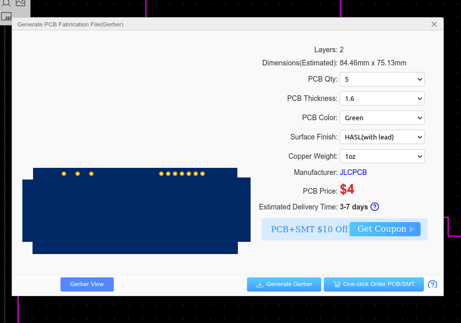</span>
But final order seems ok:


 Brand new interactions and interfaces.


 Easy to use and quick to get started.