You need to use EasyEDA editor to create some projects before publishing
PCI chamfer
638 5
Angel LaHash 3 years ago
I want to make a PCI board. I did think they where just a PCB that slots in but reading more it has a edge to split the pins a bit ![image](https://www.multi-circuit-boards.eu/fileadmin/img/03_Design-Hilfe/pc_pci-karten/pcb_pc_card_2.gif) 
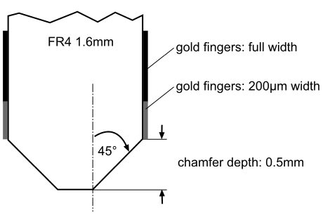
and wondering how to do that on EasyEDA
Comments
andyfierman 3 years ago
You can probably do this using a V-Cut but there are a number of restrictions on how they can be used. They must cross the whole board. They cannot start or end inside a board outline. I can't find the topic now but there was a recent post about certain conditions where V-Cuts cannot be used in panelisation to separate boards. So even though this may not be how you wish to use them, it may still restrict you if you want to panelise the boards.
Reply
Angel LaHash 3 years ago
Sadly the V-Cut isnt cutting it :( I dont understand that i see PCI Slot boards on this system and there are Footprints but it feels like they just ignored the Chamfer is it case i have to get a 1.6mm board and then Chamfer each side myself with a 0.5mm (OMG 1/2mm !!) each side making it 1.5mm at the point
Reply
andyfierman 3 years ago
You are correct: a V-Cut lone dies not cut all the way through the board. But, if you place a V-Cut line along the end of the gold PCI edge fingers then when you snap off the end of the PCB,  it will leave the 45 degree profile as shown in your picture, that you want.
Reply
andyfierman 3 years ago
"... a V-Cut line does not..."
Reply
andyfierman 3 years ago
Here's an example of using a V-Cut (not exactly the way you want but it shows what I am trying to describe): ![image.png](//image.easyeda.com/pullimage/aCg8OKyYfVaAYluwbtOLi9Niq5xRAbruMHH2Jn5P.png) The horizontal Board Outline line produces a V-Cut. The highlighted element is a vertical Multilayer Board Cutout. In other words it produces a slot in the board. So the region containing LED2 and JP17 can be snapped off along the horizontal V-Cut line leaving the part of the board to the left of the slot still attached to the main PCB (in my application this was also snapped off but that does not matter here). If you were to look closely at the snapped off edge along the line of the V-Cut, you would see something that looks like the images here: [https://www.multi-circuit-boards.eu/en/pcb-design-aid/mechanics/v-scoring.html](https://www.multi-circuit-boards.eu/en/pcb-design-aid/mechanics/v-scoring.html)<br> <br> This is almost what you want but I think you are right: you would still need to post-process the board edges to change the angle from the V-Cut of about 30 degrees to achieve a 45 degree angle. :(
Reply
Login or Register to add a comment
goToTop
你现在访问的是EasyEDA海外版,使用建立访问速度更快的国内版 https://lceda.cn(需要重新注册)
如果需要转移工程请在个人中心 - 工程 - 工程高级设置 - 下载工程,下载后在https://lceda.cn/editor 打开保存即可。
有问题联系QQ 3001956291 不再提醒
svg-battery svg-battery-wifi svg-books svg-more svg-paste svg-pencil svg-plant svg-ruler svg-share svg-user svg-logo-cn svg-double-arrow -mockplus- -mockplus- -mockplus- -mockplus- -mockplus- -mockplus- -mockplus- -mockplus-@1x -mockplus-

Cookie Notice

Our website uses essential cookies to help us ensure that it is working as expected, and uses optional analytics cookies to offer you a better browsing experience. To find out more, read our Cookie Notice