You need to use EasyEDA editor to create some projects before publishing
Pads being added to netlist by schematic->pcb converter
1106 1
nweishaar 6 years ago
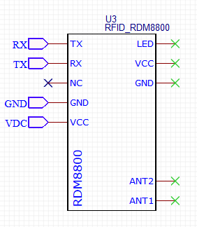
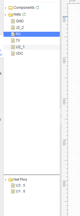
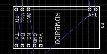
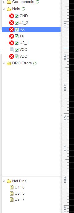
Why is my PCB editor adding pads to my netlist that aren't connected in the schematic? I'm using no connect flags and the design rules check in the schematic editor is happy and reports no errors, but when I create a PCB from the schematic, my PCB has pads in the ratsnest that are supposed to be no connect. What am I doing wrong? I can go into the PCB editor and remove the net from the pad, but then when I make a change and reimport, it is connected again and I must disconnect it again. ![rdm.png](//image.easyeda.com/pullimage/3hqDroHMhXYG1wj8UMuBmyeQ5yVUIvUkZ4ZwQxEE.png) ![schematic_netlist.png](//image.easyeda.com/pullimage/y9iE3Q0dPkLgwoioXgrvgEdxKpMGOJipD1VXST4a.png) ![rdm_pcb.png](//image.easyeda.com/pullimage/bW6vrDiXnRMhAQcbj60RwOPX9O13h0osJlJFGeRw.png) ![pcb_netlist.png](//image.easyeda.com/pullimage/FgrWQwuj0W535XYoVNkLhYFTQ2eVFHjwhDUmlcLZ.png)
Comments
andyfierman 6 years ago
The problem is that you are using a schematic symbol contributed by one user (iJackBauer) and a PCB package contributed by another (memphis) and the two have used different pin numbering. There are two problems. 1\. the two contributors have used different pin numbering\. You have to make the pin numbering on the schematic symbol match the physical pin numbering on the PCB package\. 2\. memphis has mistakenly assigned net names to the pins on the package\. This \(a\) forces pins to be connected even if you put "no Connect" symbols on them and \(b\) if the netnames assigned to the pins are different from the netnames on the connections to them then they do not connect to the external nets\. The simplest and most reliable way to fix this is to clone memphis's package and save it with a unique name. Then SHIFT+F search for it again, select and **right-click > Modify** and then add a Description including links to the manufacturer's device page and to datasheet(s) showing pinout and PCB footprint. If you cannot find manufacturer's information then please include links to the information from a reputable supplier's pages and include supplier part number. Then open the new package and delete all the netnames (and the spice pin numbers as there is no spice model for this device) applied to each pin. Then renumber the pins to match the schematic symbol. Save it. Now clone the schematic symbol. Save it with the same name as your new package. Search for it and copy and paste the Description from the package into the description for the symbol. Open the symbol for editing. Change the "package" attribute to exactly the same name as that of your new package. Save it. * Please check the schematic symbol and your new part against the datasheets and correct any errors. When you next search for the symbol, it should appear together with your package.
Reply
Login or Register to add a comment
goToTop
你现在访问的是EasyEDA海外版,使用建立访问速度更快的国内版 https://lceda.cn(需要重新注册)
如果需要转移工程请在个人中心 - 工程 - 工程高级设置 - 下载工程,下载后在https://lceda.cn/editor 打开保存即可。
有问题联系QQ 3001956291 不再提醒
svg-battery svg-battery-wifi svg-books svg-more svg-paste svg-pencil svg-plant svg-ruler svg-share svg-user svg-logo-cn svg-double-arrow -mockplus- -mockplus- -mockplus- -mockplus- -mockplus- -mockplus- -mockplus- -mockplus-@1x -mockplus-

Cookie Notice

Our website uses essential cookies to help us ensure that it is working as expected, and uses optional analytics cookies to offer you a better browsing experience. To find out more, read our Cookie Notice