You need to use EasyEDA editor to create some projects before publishing
QFN-20 DRC Pad Spacing Errors
910 12
DJDevon3 5 years ago
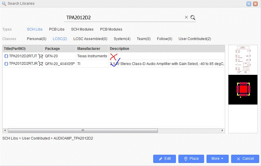
Spent a lot of time working on setting up a project using the TPA2012 only to find that the PCB puts out 16 DRC errors because the pads are not spaced far enough apart. 16 DRC pad spacing errors. The reason I used the QFN-20 was because the pinout and layout look like the real chip so naturally I figured it would be more accurate... wrong. :/ I was pulling my hair trying to figure out why I kept getting errors then it occurred to me that the package itself seems to be incorrectly designed.  Perhaps I'm doing something wrong? If it is a problem with the package then please pull it from the LCSC library.  That cost me a lot of time. Thankfully since I already designed my project around that chip it was a quick fix to drop the other package in and hook everything back up. I used the QFN-20_4X4X05P and it worked fine the first try. QFN-20 fails and the QFN-20_4X4X05P is good. I choose an LCSC option.  Apparently if I chose system it would have been the correct version. :/  Can we have a way to vote up/down or leave comments on a particular design?  Perhaps a way to report a part to admins for inspection? ![TPA2012_DRCFAIL.gif](//image.easyeda.com/pullimage/B72rG6ZWzjYl0dmDXLFoD4qJ3FrLAn2wxDdTlFSg.gif)
Comments
UserSupport 5 years ago
Hi That seems your design rule influence, can you try change the clearance smaller? ![图片.png](//image.easyeda.com/pullimage/bUb2TKkQWNwT6QtPpB1AaHXWKLWvvcjBprjwQFPU.png)
Reply
DJDevon3 5 years ago
I tested it out on 6 mil and 4 mil.  Sure enough it fails on 6 mil and works fine on 4 mil.   The weird thing about it is that's an amp so I would hope it would accept thicker traces let alone standard 6 mil traces.  I mean 6 is the default setting. I did think about decreasing the trace width but that wouldn't fix a spacing tolerance issue.  Thank you! I'll be more concise of this error in the future.  Thank you for your help!  On the bright side I have 2 different designs of the same thing now. :)
Reply
DJDevon3 5 years ago
Why would the other package work fine on 6 mil? Seems odd.  I'd rather go with the thicker spacing and thicker traces for an amplifier.  I went through about 5 different designs trying to figure out that issue.  Glad I didn't delete that project. The learning curve in EasyEDA is easy but there are nuances to every software program.  If you're not frustrated at least once a day you're not learning anything new. :)
Reply
MikeDB 5 years ago
Why they are both called QFN20 is beyond me but it is specified as lower power.  I suspect it was created for a mobile phone or something where size is important and somehow LCSC have got the surplus stock.   The larger one is the standard TI part and probably the best one to use but they are both correct.
Reply
DJDevon3 5 years ago
Smaller footprint and traces makes sense for a lower power device sure but there's no differentiation in the description.  It would have been very helpful in the package description that it requires less than a 6mil tolerance design rule. Being new to EasyEDA they looked the same to me. The only difference was the schematic design/pinouts. I went for the schematic that looked like the chip in the datasheet. :/ I really like EasyEDA so far.  It's pretty freaking awesome.  Very appreciative of the support forums.  Very fast response.
Reply
MikeDB 5 years ago
JLCPCB can go down to 3.5mil spacing if you need it so it would be possible to use the smaller pitch device.
Reply
DJDevon3 5 years ago
Figured that out after reading JLPCB setup guides after my last post.  Figured out JLPCB's minimal tolerance is 5mil and the QFN-20 works with 5 mil spacing. :) I've updated both of my designs to use 5 mil now.  Their guide is great for newbies. Is the default EasyEDA configuration for single or multi-layer PCB's?  I see my project has many layers so what constitutes a multi layer board?  One that uses vias?  Because my design has a lot of vias.  Does that mean I can go down to 3 mil if I want because I'll be using their multi-layer service anyway if vias mean multi-layer?
Reply
andyfierman 5 years ago
@DJDevon3, Could you post a link to the JLCPCB setup guides? Thanks.
Reply
MikeDB 5 years ago
[https://jlcpcb.com/capabilities/Capabilities](https://jlcpcb.com/capabilities/Capabilities)
Reply
andyfierman 5 years ago
@MikeDB, Thanks. It's not well signposted for newcomers. :)
Reply
MikeDB 5 years ago
@DJDevon3 It's 3.5mil just for 4 or greater number of layers.   5mil for a 2 (double) layer board.  Number of vias doesn't matter.
Reply
DJDevon3 5 years ago
Ah thank you Mike you're very helpful!
Reply
Login or Register to add a comment
goToTop
你现在访问的是EasyEDA海外版,建议访问速度更快的国内版 https://lceda.cn(需要重新注册)
如果需要转移工程请在个人中心 - 工程 - 工程高级设置 - 下载工程,下载后在https://lceda.cn/editor 打开保存即可。
有问题联系QQ 3001956291 不再提醒
svg-battery svg-battery-wifi svg-books svg-more svg-paste svg-pencil svg-plant svg-ruler svg-share svg-user svg-logo-cn svg-double-arrow -mockplus- -mockplus- -mockplus- -mockplus- -mockplus- -mockplus- -mockplus- -mockplus-@1x -mockplus-

Cookie Notice

Our website uses essential cookies to help us ensure that it is working as expected, and uses optional analytics cookies to offer you a better browsing experience. To find out more, read our Cookie Notice