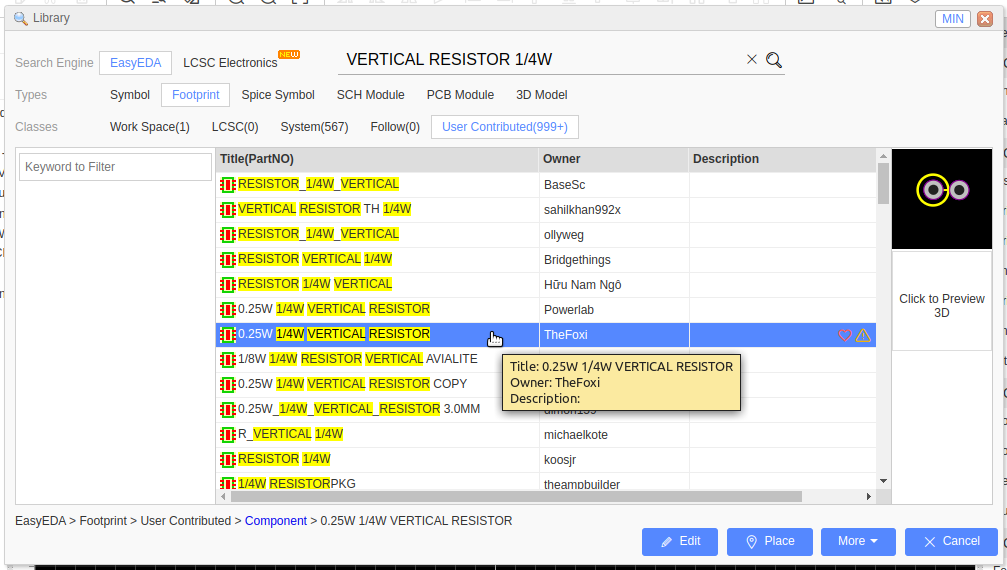
1. Find and edit or create a new PCB Footprint;
2. Save it with a unique name;
3. Place a suitable Schematic Symbol;
4. Assign the new PCB Footprint to the symbol, using the Footprint Manager.
For more, read about Symbols and Footprints in the Tutorial, (1), and then also read (2.3), in (2) in:
[https://easyeda.com/forum/topic/How-to-ask-for-help-and-get-an-answer-71b17a40d15442349eaecbfae083e46a](https://easyeda.com/forum/topic/How-to-ask-for-help-and-get-an-answer-71b17a40d15442349eaecbfae083e46a)<br>
<br>
Please also read the Footprint Naming Reference
[https://easyeda.com/forum/topic/EasyEDA-Footprint-Naming-Rule-Reference-9b470b52aeca46228b446f1fc0e323f0](https://easyeda.com/forum/topic/EasyEDA-Footprint-Naming-Rule-Reference-9b470b52aeca46228b446f1fc0e323f0)
There are **lots** of suitable footprints in the SHIFT+F Library:
****
<br>
but you **must** check the dimensions for the resistors that you have or are going to use.
You can use your own measurements but the best way to do this is to check the footprint against the original manufacturer's datasheet.
Our website uses essential cookies to help us ensure that it is working as expected, and uses optional analytics cookies to offer you a better browsing experience. To find out more, read our Cookie Notice