You need to use EasyEDA editor to create some projects before publishing
Routing failing with custom designed pads
725 5
Rodrigo Schramm 4 years ago
Hi, I am trying to create a footprint with custom pads. When I try to run automatic routing, it fails to connect. ![Screen Shot 2019-10-11 at 12.47.36 AM.png](//image.easyeda.com/pullimage/NHvnh4op4MUTgxhiwZchV7DQxBod8Utrm6WFo9rX.png) 
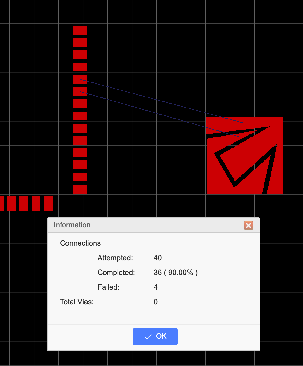
If I put these two pads away from each other, the automatic routing connects them. ![Screen Shot 2019-10-11 at 12.46.57 AM.png](//image.easyeda.com/pullimage/US1GdOwycATSHUNnfUMowcXOYTuuAgIpaC8ZnY2n.png) 
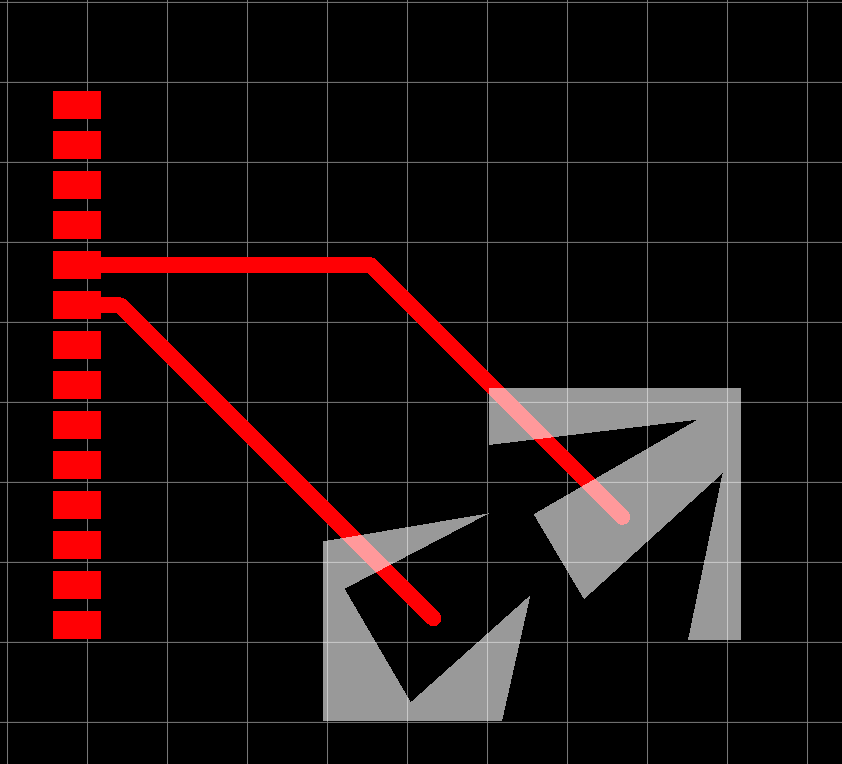
I guess the reason why it is not connecting when they are close each other is because the routing algorithm is trying to connect the center of gravity of each pad. Is there a way to fix this?
Comments
UserSupport 4 years ago
Just Routing manually.
Reply
andyfierman 4 years ago
This is essentially the same problem as I  have described in my replies to this topic: [https://easyeda.com/forum/topic/PCB-trace-antennas-seem-impossible-to-use-d4f1b45fe1e04a4187603026826c084b](https://easyeda.com/forum/topic/PCB-trace-antennas-seem-impossible-to-use-d4f1b45fe1e04a4187603026826c084b) If you read my replies and follow the links, that should help you understand the issue. You might be able to work around it by adding a small second pad with the same number on a corner of each of the irregularly shaped pads but it may still  fail due to the bug I have reported. Try manually routing out from the small pad and then let the auto router do the rest. In the antenna  case, I tried forcing the routing to avoid an area by inserting a "No Solid " area but that didn't work and probably wouldn't be possible in your  pads shapes anyway. Another way round it is to redraw the shape so that the snap area is moved to an edge or a corner. I did this with a pair of rectangular pads that I used to make the SHORTING_LINK footprint to move the two snap points to each end but I don't know if that will work with a more complex polygon like yours. It would also be harder to visualise with the points editing tool. Support mentioned turning snap off but I've not explored ways to exploit that yet. * Another possibility would be to make your pads our of several, slightly overlapping sub-pads each with the same pad number. Then the snap points will always be within some part of the overall shape and you may not care which one the autorouter snaps to.
Reply
Rodrigo Schramm 4 years ago
@UserSupport Thanks. I managed to reshape it using manual routing.
Reply
Rodrigo Schramm 4 years ago
Now I have a new problem. In fact, I am having many CLEARANCE errors on DRC check. The object in the figure below is my footprint\. I manually routed the internal connections\, and I can auto routing the footprint to the external components \(NET U3\_33 and NET U3\_34\, connected to the pads on the left part of the image\)\. However\, when I try to export the Gerber files\, the DRC complains\! I have double-checked the clearance distance and the tracks seem to be inside the limit.  Any help? ![Screen Shot 2019-10-11 at 1.34.27 PM.png](//image.easyeda.com/pullimage/chLSBFMznGYJ3R1Ou0VUKYTjKpvYCdecDAdp9uDp.png) ![Screen Shot 2019-10-11 at 1.30.04 PM.png](//image.easyeda.com/pullimage/BftUCnS8WcpQQ3ClXhoP7FNccPuRokCXR85CBgI3.png)
Reply
andyfierman 4 years ago
[https://easyeda.com/forum/topic/How-to-avoid-DRC-errors-when-connecting-to-PCB-Footprints-a-k-a-PCB-Libs-90bf944fe3644b21a7d27a9e9d8df8d6](https://easyeda.com/forum/topic/How-to-avoid-DRC-errors-when-connecting-to-PCB-Footprints-a-k-a-PCB-Libs-90bf944fe3644b21a7d27a9e9d8df8d6) [https://easyeda.com/forum/topic/How-to-create-a-capacitive-touch-pad-f6395e879953426bb6c31531553ac160](https://easyeda.com/forum/topic/How-to-create-a-capacitive-touch-pad-f6395e879953426bb6c31531553ac160)
Reply
Login or Register to add a comment
goToTop
你现在访问的是EasyEDA海外版,使用建立访问速度更快的国内版 https://lceda.cn(需要重新注册)
如果需要转移工程请在个人中心 - 工程 - 工程高级设置 - 下载工程,下载后在https://lceda.cn/editor 打开保存即可。
有问题联系QQ 3001956291 不再提醒
svg-battery svg-battery-wifi svg-books svg-more svg-paste svg-pencil svg-plant svg-ruler svg-share svg-user svg-logo-cn svg-double-arrow -mockplus- -mockplus- -mockplus- -mockplus- -mockplus- -mockplus- -mockplus- -mockplus-@1x -mockplus-

Cookie Notice

Our website uses essential cookies to help us ensure that it is working as expected, and uses optional analytics cookies to offer you a better browsing experience. To find out more, read our Cookie Notice