You need to use EasyEDA editor to create some projects before publishing
Solid region with exposed copper cannot be deleted
1738 8
amsgomes_9956 4 years ago
Andy . 
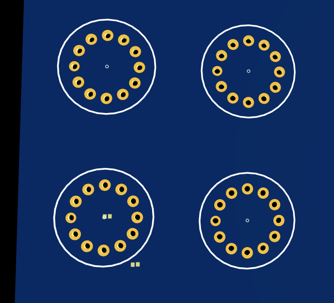
I drew a solid region (4 squares) and set it as exposed copper. Then I gave up to have  these solid regions and deleted them and drew other stuff on that place of the board. I noticed that the solid regions that I deleted still appear in 3D view and in the Gerber file. I am attaching the pictures showing the problem. ![tela1.png](//image.easyeda.com/pullimage/I3eYRElZjsYH78ugbDGCbe71Vpmi1XSMnTbKO4Hq.png) in the next image, from 3d view, look at the bottom left circle where 4 small solid rectangles appears. ![tela2.png](//image.easyeda.com/pullimage/g40Kjhn2cDdCUVALcM5Ch5CBh3lJvj5D1L2Rt11C.png) 
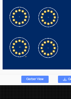
Now the screen that shows the gerber file to be sent for production: ![tela3.png](//image.easyeda.com/pullimage/LoauronycjxkJ4DaXldEk20FqqFNtDSRCCxLjbD6.png) NO matter what I do, I cannot remove the squares from the pcb layout because they were already deleted. I cannot find them anywhere on pcb layout. 
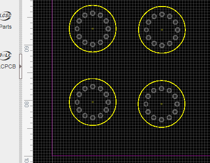
the pcb layout is BottomBoardV2 in my project. How can I fix this ?
Comments
andyfierman 4 years ago
When you click expose copper for a solid region, apertures are created in the associated solder mask layer Have you deleted the apertures in the relevant solder mask layer?
Reply
amsgomes_9956 4 years ago
Hi Andy, sincerely I don't remember. For me, to delete something I just need to select it and click delete. But ok, in a case where I did not delete such "apertures" (I still don't know what it means), how do I select these forgotten apertures now and delete them. I cannot see "apertures" or "square" in any layer or object window.
Reply
amsgomes_9956 4 years ago
Andy. I did solve my problem, but in a HARD way. The steps I performed: 1\. Rename the PCB saving it with another name \(BottomPCBV2 to BottomPCBV3\) 2\. Select only objects that I want and then copy \(control\-C\) 3\. Go to the pencil icon and click Global Delete 4\. Restore the objects with Paste \(control\-V\) 5\. Save the fix pcb layout \!\!\! Of course, this is a workaround for my problem, but I would appreciate if you can tell me how to fix the problem without performing a Global delete. Althoght I think it is a real bug in PCB layout. As you can see in step 1, the former pcb is still in my project in case you need to check what was going on, I will work on the V3 version from now. Regards.
Reply
pinoccio 4 years ago
Form me a simple solution worked: select and Ctrl+X the whole PCB, then Ctrl+Z (undo the step) - resulted in just removing the solid copper area.
Reply
UserSupport 4 years ago
please check have you deselect the component at design manager?
Reply
dorio80 3 years ago
Andyfierman is right. This happened to me too when I exposed copper on a track. I changed my mind and wanted to un-expose it, but there is no control for doing that. Also my solder mask layers were not enabled in my layer manager. Once I enabled them I could see the apertures Andyfierman is talking about and could delete them. Of course there were multiple ones because I tried to un-expose the tracks by clicking the same button and every click created a new aperture. Sorry to revive an old thread, but I thought someone else would wonder where these apertures are. By default my solder mask layers were not enabled.
Reply
kartick ravi 1 year ago
just select the top/bottom soldermask layer and delete it ;)
Reply
andyfierman 1 year ago
@karticravi, To clarify: Sorry but the advice to: "just select the top/bottom soldermask layer and delete it" is unclear at best and dangerous at worst. You do **not** want to delete the **whole** Soldermask layer: just specific apertures in it. Turn off visibility of all layers except the desired top/bottom Soldermask layer (and the associated Silkscreen layer to help identify the desired aperture); This will then show the apertures in the selected Soldermask layer; Select and then delete the aperture(s) as required. Note that apertures may need to be unlocked in the right hand panel (or Right-Click > Unlock) before they can be deleted.
Reply
Login or Register to add a comment
goToTop
你现在访问的是EasyEDA海外版,使用建立访问速度更快的国内版 https://lceda.cn(需要重新注册)
如果需要转移工程请在个人中心 - 工程 - 工程高级设置 - 下载工程,下载后在https://lceda.cn/editor 打开保存即可。
有问题联系QQ 3001956291 不再提醒
svg-battery svg-battery-wifi svg-books svg-more svg-paste svg-pencil svg-plant svg-ruler svg-share svg-user svg-logo-cn svg-double-arrow -mockplus- -mockplus- -mockplus- -mockplus- -mockplus- -mockplus- -mockplus- -mockplus-@1x -mockplus-

Cookie Notice

Our website uses essential cookies to help us ensure that it is working as expected, and uses optional analytics cookies to offer you a better browsing experience. To find out more, read our Cookie Notice