You need to use EasyEDA editor to create some projects before publishing
"Thermal pads" in footprint identified as vias in DRC
581 3
THX1138 2 years ago
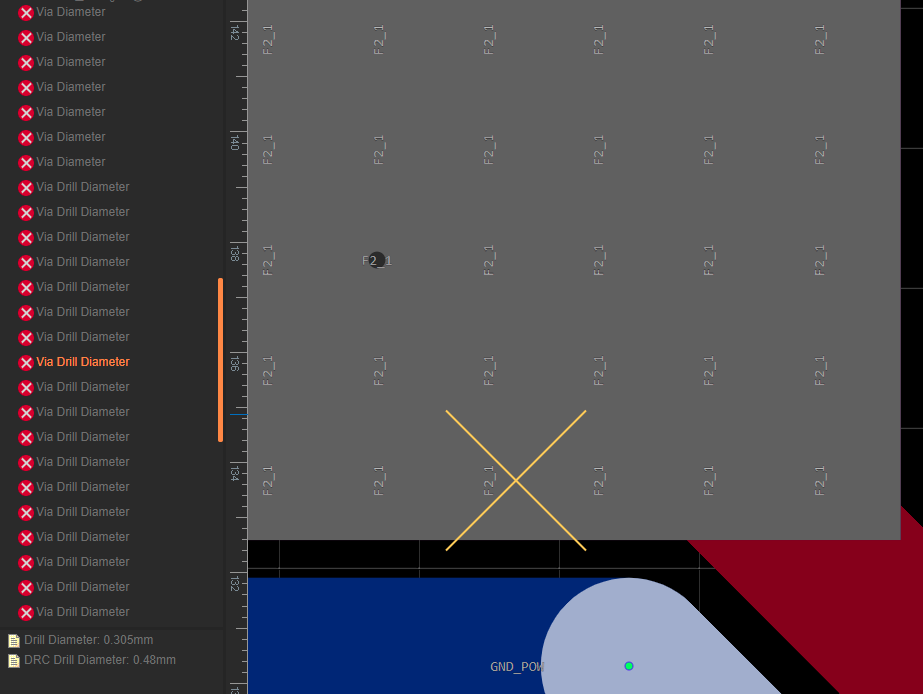
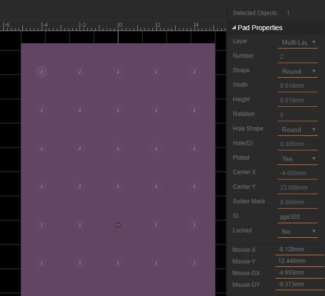
I wanted an area for a TO-220 component to be soldered to the PCB and cooled. I modified a footprint to include one really large rectangular pad and put lots of small circular pads inside it (diam 0.61 mm, hole 0.305 mm). I updated the footprint of my component in the schematic and updated the PCB to include the modified footprint. The pads are identified as vias and trigger the DRC, even though they were created as pads and shouldn't need to obey the design rules for vias because a) they're for heat, not power and b) there's 45 of them anyway (generating 90 DRC errors). For some reason the PCB view doesn't show the holes in the centre of the thermal pads even though the holes are present in the 3D view. I think EasyEDA should just add a feature for making thermal vias which are exempt from the normal rules for connections and diameter etc. [https://easyeda\.com/editor\#id=\|bceeb9c3354e4eefb7b1aebc1d7b3105\|53b8858434d0471e8478ad83bd7a6130\|beacd93fad4a40a3b592bb6dc4595450](https://easyeda.com/editor#id=|bceeb9c3354e4eefb7b1aebc1d7b3105|53b8858434d0471e8478ad83bd7a6130|beacd93fad4a40a3b592bb6dc4595450) ![image.png](//image.easyeda.com/pullimage/IY6TLbWIbjQtGVkQnfqMjhkQfClZsrpzYWeV8JhY.png) ![image.png](//image.easyeda.com/pullimage/NSqimVS889dGEGeqll7RIlzcaYRHsOYa083uhjtd.png)
Comments
deskpro256 2 years ago
Hi! No problems with EasyEDA here as far as I'm concerned. You seem to have messed up with the vias! Easy mistake. When you check the design rules, you can see that the net F2_1 is in "High power" rule. But the vias you have there are for the "Low power". ![Screenshot_1.png](//image.easyeda.com/pullimage/pQJvt35xcgQmPoGMeX0T3pj3StuOsZ5rjx0W7jM5.png) To fix that easily, select one of the vias, right click on it, then select "find similar objects". In that menu most things will be already set, but change the net to F2_1 and press find. It will select all the vias there and then just change the via parameters in the right side properties box. ![Screenshot_2.png](//image.easyeda.com/pullimage/otjmmnm19BSWjjyKIgCQWbc3TMAZDFCVgar0LMNL.png) When that is done, you can check the DRC again and there should not be any problems with those vias anymore. The other thing with the clearance\. The Copper layer you have on the bottom layer is a different net\. U1\_3 and the top layer and the vias are U3\_3\. To fix that\, select the bottom copper area and change the net to U3\_3: ![Screenshot_4.png](//image.easyeda.com/pullimage/XzrsDM85Etz8LtnhZywXVLPuYZvuxCwXnkewFZYW.png) On to the next thing: The trace width errors are for you to fix. The current width for the traces is 2,4mm and 3,2mm. The 2,4mm are too small for your 3mm rule. Either change the rule or the traces. By quick calculations using Saturn PCB calculator, these traces are able to handle about 6A, are you sure you need that much? What voltages will be there? No silk screen text is there to help connect wires to the PCB. What is VCC? Also the traces are far away from your loads, the voltage drop on that trace would start to be a pain in the ass for that length. Re-think that. And ~~a lot of~~ all the routing needs to be re-done. The autorouter has set you up for a big failure. Try to route all of this by yourself and also have a go at re-trying the component placement and rotation. Maybe there is a way to get it looking neater. Also, even if you do choose the autorouter way, don't let it route the GND, it will screw you up big time. The schematic is also a big mess. Keep everything in the sheet to later print it out. If you can't get it all on one sheet, use another sheet for things. Make separate sheets for the microcontroller with the OLED and buttons and another for the control circuits. The way you have a lot of things on top of each other and just a general mess, it is really hard to look at it. Feel free to check out other peoples projects and see how you can improve your work. Do you have a case in mind that you will use or will you make it around the PCB. I'd suggest you find a case and then make the PCB for it. Saves a lot of time. You can check out Robert Feranec or Dave from EEVBlog on youtube, they have good and entertaining videos about these things. Here I have made a project with the schematic in two sheets and the PCB made for a particular case. It's not perfect, but can help you see different [https://easyeda\.com/editor\#id=b8e7083d5751488c87a9dc30c1ca53c0\|e44b983558264cacae7d238292e789fb\|cc6a4065c47f4b5780e4c52cbdcb411e](https://easyeda.com/editor#id=b8e7083d5751488c87a9dc30c1ca53c0|e44b983558264cacae7d238292e789fb|cc6a4065c47f4b5780e4c52cbdcb411e)<br> <br> Hope this helps you finish your project even better!
Reply
THX1138 2 years ago
Hi. Thanks very much for all your feedback. It's going to take a while to overhaul the layout but I'll post again at some point when it's done. For the enclosure, I want this to be thin since it will be wearable - it's a thermostat for my 12 V, 5 A heated clothing project - I intended to design PCBs to match the front and back and attach them using screws and standoffs. I could alternatively just laser-cut some thin acrylic though. I did use the autorouter but I spent several hours (it's my first time) adjusting the tracks to separate the signals. I think the only sensitive signals will be the ones for the display. I'll make sure to read the current sensor and thermistors a certain time after the MOSFETs have switched so they won't experience interference from that.
Reply
THX1138 2 years ago
I changed the layout and routed everything manually. I'm not sure I'm much better than the auto-router though. At least it didn't take any longer than using autorouter and then fixing autorouter's routes. [https://oshwlab.com/THX1138/arduino-nano-thermostat](https://oshwlab.com/THX1138/arduino-nano-thermostat)<br> <br> I'm not certain what to do about the fuses. Since I want the project to be thin and wearable under additional clothing, I would really like to replace the THT fuses with SMD ones (of course the THT ones were going to be folded over but they're still bulky even then). In the case of the main fuse, I'd have to use two in parallel to provide enough current and I also have to think about the amount of heat coming out of the dual diode (I expect 1.25-1.8 watts at 5 A, depending on how hot the diode gets) and the thick tracks will send it straight to the fuses which will be producing a fair amount of heat themselves. I might put two 4 A fuses in series, since the heat will reduce I(hold). Then again, there's always some distance between I(hold) and I(trip) anyway. I could also use a conventional FF glass fuse instead. ![PCB_v2_PCB_Arduino Nano Thermostat_fixed_FPC_moved_GND5A_D1_footprint_2021-09-25.png](//image.easyeda.com/pullimage/uTVxET0FbNmTJI9A72sH7Qv7uxAZi5O9sEE3DntX.png)
Reply
Login or Register to add a comment
goToTop
你现在访问的是EasyEDA海外版,使用建立访问速度更快的国内版 https://lceda.cn(需要重新注册)
如果需要转移工程请在个人中心 - 工程 - 工程高级设置 - 下载工程,下载后在https://lceda.cn/editor 打开保存即可。
有问题联系QQ 3001956291 不再提醒
svg-battery svg-battery-wifi svg-books svg-more svg-paste svg-pencil svg-plant svg-ruler svg-share svg-user svg-logo-cn svg-double-arrow -mockplus- -mockplus- -mockplus- -mockplus- -mockplus- -mockplus- -mockplus- -mockplus-@1x -mockplus-

Cookie Notice

Our website uses essential cookies to help us ensure that it is working as expected, and uses optional analytics cookies to offer you a better browsing experience. To find out more, read our Cookie Notice