You need to use EasyEDA editor to create some projects before publishing
Top / Bottom layer and autoroute
2425 10
Steve Lee 5 years ago
Hi 
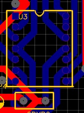
Is there a way to design a pcb lib package that has bottom only layer connections but the component itself will sit on the top? The problem is if you set all the connections just to bottom the auto router will place tracks across the components connections on the top layer. This is fine for smd components but doesn't work for something like a pdip carrier socket where the connections are always onto the bottom layer but the socket itself is sitting on the top layer and has connections through the pcb. To illustrate see pin 7 (bottom left) in the attached. All the sockets connections have been set to the bottom but a track is going through pin 7 on the top effectively giving a  connection between the top and bottom layers where it shouldn't. A similar problem occurs with the auto router if you mark connections to an ic in a schematic as n/c. The auto router then believes its fine to place a track through the n/c pin when in reality although the circuit design may purposely have no connection internally inside the ic the pin may actually do something! The work around is not to mark pins as n/c in the schematic but that makes having a n/c element pretty pointless. ![pin.jpg](//image.easyeda.com/pullimage/DoeCwBich408gozR1G61LL27W5Y3FZlExdGnUziw.jpeg)
Comments
andyfierman 5 years ago
That is not the right way to make a PCB footprint for a through hole component whether it is a socket or an component such as an op amp or a resistor. EasyEDA is a multilayer PCB tool and the default number of layers of the tool and JLCPCB's PCB fabrication is 2 layers: top and bottom. More layers can be specified in the PCB Layer setup. Pads for through hole footprints are called Multi-layer. * Any multi-layer pad therefore has a pad on the top and a pad on the bottom (plus on all other layers that may be specified in the PCB Layer setup) and those pads are joined by copper plating inside the hole. These are called Plated Through Holes (PTH). So for example, a PCB footprint for a 14 pin DIP as in your image will have 14 pads on the top layer and 14 pads on the bottom layer with each top and bottom pair joined by their associated through hole plating. If you want to route between the pads of a PCB footprint on any layer then you have to set the track width to be no wider than the spacing between the pads less twice the clearance set for that class or family of nets. If you rely on the autorouter then you may have to set all your tracks to meet the above criteria which may limit their current carrying capacity in some cases. If you hand route your critical nets then you can hand edit the track widths as they pass between pins then let the autorouter finish the routing.
Reply
Steve Lee 5 years ago
Thanks for the detailed reply Andy much appreciated I am actually doing what you suggest i.e. hand routing my critical nets either prior to or when possible post running the autorouter. This works fine I was just hoping there was a way of saving more time. The problem with setting the DIP pads to multi-layer is it then makes it simply impossible to solder to any top layer tracks the autorouter creates as the physical DIP socket covers the top pads hence why you really need to have all the connections on the bottom. The same thing can apply to other components such as PCB mounted sockets where, when placed on the board, the physical socket covers the top pads making soldered connections to those pads impossible. The good thing is a DRC check will pick out the instances where the problem I showed in the image occurs so you can the manually edit the tracks to resolve things it would just be great if the autorouter did it for you!
Reply
andyfierman 5 years ago
"The problem with setting the DIP pads to multi-layer is it then makes it simply impossible to solder to any top layer tracks the autorouter creates as the physical DIP socket covers the top pads " Not true. You have not understood the significance of PTH. Because the top and the bottom layer pads are shorted together by the PTH you only need to solder to the bottom side of the PCB. There is a good set of diagrams to illustrate PCB construction here: [https://www\.pcbway\.com/helpcenter/technical\_support/What\_a\_PCB\_Is\_Made\_Of\.html](https://www.pcbway.com/helpcenter/technical_support/What_a_PCB_Is_Made_Of.html) If you are making your PCB by hand etching or CNC milling then that is a different matter. Whilst it is possible to do this, as you can see, it creates an additional workload with extra possibilities for errors. * We do not recommend DIY etching or machining to produce PCBs since you have no means of through plating holes.
Reply
Steve Lee 5 years ago
@andyfierman Thanks Andy but I really must be missing something somewhere\. So if on the DIP socket I make all the pads plated multi layer ones then yes there is a connection between the top and bottom and all connections can go through the bottom\. That however isn't the problem\. Referring back to my original image where the pads \*are\* all multi\-layer and plated and the autorouter has made the correct net connection to the bottom layer why is it in placing a track from a totally unrelated net through the same pad on the top layer? Given the pad is plated then surely the autorouter should recognise there is a connection between the top and bottom of the pad and avoid placing a track through the top? I've proved the width of the track doesn't seem to solve the behaviour\. Another example if I place a PDIP package ic (so an ic where the pins are through the hole) on a schematic and then say mark 4 sequential pins as n/c then convert to a pcb and run the autorouter then in many cases it will place a track (or tracks) through all 4 pins on the top layer that have been marked n/c i.e. the act of marking them n/c seems to tell the autorouter that the pins don't exist at all. I apologise if I'm missing something obvious! I'm just a recently returned hobbyist who makes & etches their own pcb's using the laser printer transfer method. I'm getting back into electronics for the first time in decades (late 1970's when a teenager and 7400 chips were newish). EasyEDA is really great and I'm just trying to get to grips with the finer details.
Reply
andyfierman 5 years ago
I can't tell what might be wrong just from your screenshot and your project is public so only you can see it. Can you make your project public or make me a Team member so I can have a look?
Reply
Steve Lee 5 years ago
@andyfierman So I'm confusing myself now! To show you the problem I'll need to clone the project as the way its set up at the moment has manual edits that are getting around the issue and I have PCB's I'm making based on it. I'll put something together for you and let you know. Anyway out of the two issues I've reported the way I've described the following one is correct. "Another example if I place a PDIP package ic (so an ic where the pins are through the hole) on a schematic and then say mark 4 sequential pins as n/c then convert to a pcb and run the autorouter then in many cases it will place a track (or tracks) through all 4 pins on the top layer that have been marked n/c i.e. the act of marking them n/c seems to tell the autorouter that the pins don't exist at all" It mostly occurs if there are many connections to the connected pads of the PDIP IC i.e. when the autorouter has to work hard to find a route - it appears to, in the end, place tracks over the n/c pads as if they don't exist when no other route can be found. The way I described the other one in the last post is wrong so many apologies. If you use plated multi-layer pads then the autorouter correctly routes to the top and the bottom pads without an issue. The "problem" occurs when you set all the pads to bottom only. In this case you can image that the DIP socket itself is forming the plating between the top and bottom layer as you have drilled a hole from the top to solder to the bottom. The autorouter then has a habit of placing tracks through where the DIP pins emerge on top. Thinking about it this isn't really a bug as this is the behaviour you'd expect from a normal bottom only mounted smd component i.e. in that case it would be fine to have tracks running across it on top (in the same way its fine to have bottom tracks underneath a top mounted smd component). The problem is simply when you need to mount the component on top but want to force all the connections to the bottom.  As I've mentioned for a DIP socket you cant get your soldering iron to do a top pad connection so if you make the DIP socket pads plated multi layer and the autorouter puts a track to a top layer pad you can't solder to it. I've actually tried designing packages where I make the pads plated multi-layer and then try and force the autorouter never to connect to the top by surrounding the pads with either a a rectangle of track of a rectangle of silk layer drawing but then set to the top layer i.e. the autorouter should never be able to find a way of connecting to a top pad. All my attempts so far just end up with the autorouter window emitting weird error messages! Is the autorouter source code opensource? As a software engineer I'm quite intrigued as to how it works. Thanks for your answers and apart from this one minor irritation I'm really pleased with EasyEDA.
Reply
andyfierman 5 years ago
" it appears to, in the end, place tracks over the n/c pads as if they don't exist when no other route can be found." No reason for it not to do that if you've marked the pins in the schematic as nc. If you place pads single layer pads these are intended for and parts. Do not put holes in them and try to use them as single sided through hole pads. That creates exactly the kind of chaos you are seeing. If you have through hole parts then create or use pads and footprints made with multi-layer pads. If you have and parts then create or use pads and footprints made with single layer smd pads. Do not try to work around these rules unless you know exactly what you are doing and the possible consequences. :)
Reply
andyfierman 5 years ago
"No reason for it not to do that if you've marked the pins in the schematic as nc." Actually I that's not quite true. There's a difference between a pin marked "Not connected" or "Unconnected" and one marked "No connect" or "Do not connect". The former are pins that could be connected to because they are not connected internally in the package. The latter are pins that may be connected internally in the package but are only for use during factory testing and must be left unconnected in normal use. Such pins are not normally described so the consequences of connecting to them are unknown. The schematic green No Connect cross symbol only means that nothing is to be connected to the pin. It has no mechanism to distinguish between "Not connected" or "Unconnected" and  "No connect" or "Do not connect" pins. If the Autorouter is routing across pads that have had No Connect symbols attached in the schematic then that certainly is a bug. Looking at your picture however, I don't think that is what's happening. I can't look at your project for a few days as I'm away with only a smartphone. Maybe someone else can have a look.
Reply
Steve Lee 5 years ago
"If the Autorouter is routing across pads that have had No Connect symbols attached in the schematic then that certainly is a bug." Yes that's what I'm seeing. It's a different issue to the one in the image. I think I may have it in an archived project that does it so I'll look at make it public. The more I think about the other issue - call it the "can't solder to a top pad of a DIP socket" then the more I realise this is a feature request and not a bug. Effectively if you set a components pads to "all bottom" (or "all top") then the autorouter assumes its rules should be for smd components which is fine. What I'm really after is a way of saying to the autorouter "even though the pads are multi-layer please only make connections to the bottom pads only"
Reply
andyfierman 5 years ago
You can specify individual pads to be NPTH but I'm not sure if that can be done for pads in a footprint or when building a footprint. I might be wrong but I don't think having pads on top and bottom but with no through plating is standard industry PCB practice other than in DIY boards. It has other implications when there are more than 2 layers. It also has negative impact on the reliability of PCBs made that way.
Reply
Login or Register to add a comment
goToTop
你现在访问的是EasyEDA海外版,使用建立访问速度更快的国内版 https://lceda.cn(需要重新注册)
如果需要转移工程请在个人中心 - 工程 - 工程高级设置 - 下载工程,下载后在https://lceda.cn/editor 打开保存即可。
有问题联系QQ 3001956291 不再提醒
svg-battery svg-battery-wifi svg-books svg-more svg-paste svg-pencil svg-plant svg-ruler svg-share svg-user svg-logo-cn svg-double-arrow -mockplus- -mockplus- -mockplus- -mockplus- -mockplus- -mockplus- -mockplus- -mockplus-@1x -mockplus-

Cookie Notice

Our website uses essential cookies to help us ensure that it is working as expected, and uses optional analytics cookies to offer you a better browsing experience. To find out more, read our Cookie Notice