You need to use EasyEDA editor to create some projects before publishing
Trying to attach PCB image to Schematic Image, getting this, what did I do wrong?
888 19
Joseph Massimino 5 years ago
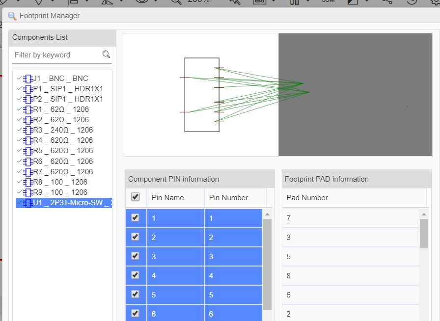
I created a PCB image, but when I go to attach it to my Schematic imager, I get this. It appears to have something wrong, even though when I look at the PCB image, it looks OK.  I'm sure it is some setting I did not set properly. I also was annoyed that I can not update a PCB  image that I saved, and made some corrections to. This explains why I sometimes get user parts that are garbage, let a user update parts that he or she contributes. OK, so I raised two points, but one can be corrected, and the other is simply a critique of the part creation process that I think is flawed. ![PCBImage.jpg](//image.easyeda.com/pullimage/ZvUQ2bpu9UXDNPjELcG4gWm9cedDRDXKl3932eNQ.jpeg)
Comments
andyfierman 5 years ago
Can you take two screenshots? One of where the schematic symbol is in the Search Library and one of where the PCB footprint is in the Search Library?
Reply
UserSupport 5 years ago
Hi Some part's image will show so small in the footprint manager, you can click the footprint view window and scroll the wheel to zoom in. this issue is waiting for improve.
Reply
Joseph Massimino 5 years ago
I managed to get it done, then printed a 1:1 pdf of the board and the part fit.   I think the User Support was right, the part I created was too small to be seen, but the second time I did it it was ok. I have a very good foot print for an E-Switch EG-2310  2P3T micro slide switch.  I'm just not sure how to keep my parts private, since they get difficult to find once I put them out for anyone to see.
Reply
andyfierman 5 years ago
@joe.massimino, "I'm just not sure how to keep my parts private..." I thought that you could keep parts private by putting them into a Team which had only you in it but I have just checked that and it does not seem to be the case. So, as far as I know, there only 2 ways to do this at present are: 1. Create your parts then paste them into a private Schematic sheet or a PCB sheet and then you can copy and paste them into other sheets as you wish. You then have to delete the parts from the Shift+F library because anything in there is public. 2. A really clumsy way to do it: Download the EasyEDA Source file for every Schematic Symbol and PCB Footprint that you make and so keep a local copy. To use it you would have to upload the EasyEDA Source file, open it in the Schematic or PCB Lib Editor and save it every time you needed it again. Once you have finished placing the parts you then have to delete them from Shift+F library because anything in there is public. "...since they get difficult to find once I put them out for anyone to see." This is exactly why - as I have pointed out in previous posts - giving your parts a clear, unique name is so important. It's like setting a password: it needs to be unique and you have to be able to remember it. Adding Tags to your personal parts is also very helpful. Now, in your case I suspect you don't actually care about making your parts _**private**_. What you really care about is being able to **find** them. That is easy. All the parts you create are listed in your User Center > Libraries > Created > Schematic Libraries or PCB Libraries and you can also filter them by the Tags: ![image.png](//image.easyeda.com/pullimage/M6XaYnioWj2yVMejTBI6pdclXp1Or5Zoa6Gytc4b.png) The same parts also appear under the Personal tab in the Shift+F Search Libraries tool under Types: SCH Libs or PCB Libs > Classes: Personal: ![image.png](//image.easyeda.com/pullimage/tvIMCbf951DN760KIHxu1plkaRqjMe8HVu4P4WKF.png) and hovering over the Personal Classes tab then shows all the Tags that were attached to the part when it was saved to the library so that it is possible to filter the search results using these Tags: ![image.png](//image.easyeda.com/pullimage/8ECRazDtPFoExxZTtBmBjIomRdUv8HS9IsmiDGxk.png) As I have said to you many times before, you need to take time out from trying to create an actual projects and just create a dummy project, the sole purpose of which is to play with the tools and learn how to use them. Learning through play is a powerful technique and is not just for kids! :)
Reply
Joseph Massimino 5 years ago
I found that once I create the part, i can't overwrite any corrections to it, and it is out where anyone can get it. What sense does that make, if I create the part, i should be able to overwrite it, or delete it.   EasyEDA does not do enough to add perfect parts to the library, they depend on the users to populate the parts, and that leads to all sorts of problems for new users to the system.   One warning I would give new users is to inspect all parts very carefully, and don't bet they are correct until you do that. EasyEda does a lot to make the software work in many ways, but parts are key to success in using the software.   It took me awhile to create my switch footprint, and make it work the way the schematic showed it. Now it works perfectly, as I printed it 1:1 and poked holes with a pin, then inserted the switch.  One part, the Amphenol BNC did not fit in the way the PCB image appeared, i would not have known that unless i did what I did, and saw that it overhung the board too much, so I pulled it back , and checked it again. That is one part I took from the library, and it could cause someone to ruin a bunch of boards. If the BNC is out too far, the mounting holes, if there are any, will not line up with the case. That is one way in which using the parts library can be a big problem.  I will try what you suggest, but I am not betting that I can delete anything. When I kept failing to make the switch PCB image, I kept trying to overwrite the same name, as i kept trying to figure it out, but NO, I could not overwrite the part. That explains why there was so much crap that is mis-labeled, and simply wrong, when I search for parts, users call their parts anything they want, no matter what makes sense to most.  They use abbreviations that they think makes sense, but those abbreviations are sometimes common to identify common parts that have no resemblance to the part the user created. So as you look through all the parts with a common term, you can find all sorts of things that have no bearing on what you are searching for.
Reply
andyfierman 5 years ago
@joe.massimino, I understand your frustration with the problems you are having with creating and editing parts but I do not understand why you are having an issue with being able to edit parts that you have created. Earlier I asked you if you could take two screenshots of the part you are having trouble editing: One of where the schematic symbol is in the Search Library and one of where the PCB footprint is in the Search Library. 1. Can you do that so I can look at the parts you have created to get some idea of what the problem might be? 2. Can you do the same for the Amphenol BNC connector?
Reply
andyfierman 5 years ago
If this is the project that you are discussing: [https://easyeda.com/joe.massimino/20db-attenuator](https://easyeda.com/joe.massimino/20db-attenuator) then at least part of the problem is that the BNC connector is not specified in the schematic (i.e. the Supplier and Manufacturer attributes have not been set) and therefore there is no way to check if the PCB footprint that you have assigned to the Schematic Symbol is correct.
Reply
Joseph Massimino 5 years ago
I will try to edit the BNC with my own PCB image, or just make my own from scratch.
Reply
UserSupport 5 years ago
If you want to assign the package for the lib, you can refer at: [https://docs.easyeda.com/en/Schematic/Footprint-Manager/index.html](https://docs.easyeda.com/en/Schematic/Footprint-Manager/index.html) if you confuse at the private lib you can refer at: [https://easyeda.com/page/contribute](https://easyeda.com/page/contribute)
Reply
andyfierman 5 years ago
@joe.massimino, "I will try to edit the BNC with my own PCB image, or just make my own from scratch." If you do that you must name it with the manufacturer's part number and put into the right-click-Modify Description field the details of exactly which manufacturer's physical part number and datasheet, your PCB footprint is designed from. Otherwise, you will have added yet another undocumented footprint to the user contributed library that no-one will be able to identify, which is after all one of your major points. :)
Reply
andyfierman 5 years ago
"One part, the Amphenol BNC did not fit in the way the PCB image appeared, ..." Why would you expect it to fit? There is no reason to suppose that the PCB footprint you have arbitrarily chosen from the library was designed to fit the Amphenol BNC connector that you have chosen from a supplier. The PCB footprint in the library has no manufacturer, supplier names or part number information assigned to it so you have no idea from which physical part it was designed.
Reply
Joseph Massimino 5 years ago
I've learned to check everything from the parts library, even if it says it is a specific part, there is no guarantee that the person who measured, and made the part did it correctly.  I am at the last stage of this project, I have some duel sided circuit boards coming with 1/2 oz copper, which I will use to prototype the circuits to work out the last changes they may need. I have one part of an amplifier that I might change from a fixed resistor , to  potentiometer. I already accounted for turning the sound off, but not adjusting it, and I can see that it might need to be adjusted.  This project has taken the longest, but it is the most expensive project I've ever done. I actually tried to etch the image to a 2 oz copper board, but it takes too long, and the resist on the pads does not hold up as well over that long etch time. So 1/2 copper will etch pretty fast, and that should give me good clean lines where the circuit is tight.
Reply
andyfierman 5 years ago
I still don't understand why you don't just get a small quantity (5 off) PCBs made via EasyEDA then you wouldn't have to be wasting your time with messy and possibly dangerous and toxic etching chemicals which you then have to dispose of responsibly.
Reply
Joseph Massimino 5 years ago
I do know how to neutralize the acids so they no longer present a problem when i am done.   The issue with the trying to work both switches into my schematic continue, but I will post a new message to explain it.
Reply
Joseph Massimino 5 years ago
@andyfierman  If I want to arrange pin numbers  on the switch, and I created the PCB footprint, but I also created the schematic drawing, and the numbers need to be changed, at what level do I go back to to rearrange  the pin numbers so they autoroute properly?
Reply
andyfierman 5 years ago
Since you have still not given us the information I asked for a couple of times about your switch symbol and footprint, I can't look at them to advise exactly what you need to do so below is a list of the steps you have to go through to (A) fudge it by only fixing your schematic and leaving a dud symbol and/or footprint in the library or (B) fixing the symbol and/or the footprint in the library. A) To fix it in the schematic, as shown in the video below: 1) First get the component datasheet out for reference. 2) Go to the schematic. 3) Select the switch symbol. 4) Click on the package attribute in the right hand panel. 5) Swap the Component pin numbers about until they match the PCB footprint. ![pin_swap.gif](//image.easyeda.com/pullimage/gppgKhH0ptw51tEKgW0CXYFhVHkUxZ5Pe3F4RLah.gif) B) However, so that no-one else can pick up your wrong part from the library, you need to permanently fix whichever is wrong out of the symbol and/or the PCB footprint in the library. 1) First get the component datasheet out for reference. 2) Then, in the Search Libraries tool, search for, select and then Edit whichever of the symbol and/or the PCB footprint you need to edit, in the appropriate Schematic Lib Editor or PCB Lib Editor. 3) Redefine the pin numbers in whichever of the symbol and/or the PCB footprint you need to fix, then Save them. 4) If you changed the Schematic Symbol, then **Update** the symbol in the schematic: ![image.png](//image.easyeda.com/pullimage/rSCC7bbVTsxCRRrN1DwGdMHwJRUcLSpPMBqQQwjm.png) 5) If you changed the PCB Footprint then do **Update PCB...** to bring the new PCB footprint into the PCB.
Reply
Joseph Massimino 5 years ago
I'm sorry for not getting back to you, I did figure it out, and I printed the image I made and etched it into a small board and my part fit, so that is good. I wanted to make two images for two different switches, but that was proving difficult, until i figured that it had to be a whole separate project. So I am thinking about what you said about making only a few boards to check it out. The part of that which is troublesome is that the shipping on 10 boards is not so much more thn 100 boards, and 100 is not so far from two hundred. The shipping is what cost the most. Then it sits in customs for a week. I don't know what the cost on 10 boards will be without making out the order, but I think I have a chance to cancel along the way, so I may do that.
Reply
andyfierman 5 years ago
@joe.massimino, Going back to your original post in this thread, the reason you have what appears to be an invisible footprint is because you have placed several partial footprints very widely scattered about the PCB Lib Editor canvas. 1. There's one centred at: X=8220.443mm, Y=-731.737mm. Some of the pins on the symbol are mapped to pads on this footprint. 2. There another partial footprint centred at: X=9074.112mm, Y=537.419mm. Some of the pins on the symbol are mapped to pads on this partial footprint. 3. And another partial footprint centred at: X=23026.334mm, Y=2552.740mm. I don't think any of the pins on the symbol are mapped to pads on this partial footprint. This is your footprint at: [https://easyeda.com/editor#id=!f0dfb346a9454ecface054dd9f6ab9e6](https://easyeda.com/editor#id=!f0dfb346a9454ecface054dd9f6ab9e6) Please delete it! As explained earlier in this thread, to avoid populating the User Contributed libraries with incorrect and incomplete symbols and/or footprints please also use the **Shift+F Search Libraries** tool (also accessed via the **Libraries** button in the left hand panel) to find and delete all your other incorrect and incomplete footprints. You will find all the symbols and footprints that you have created on your page under the Libraries heading: ![image.png](//image.easyeda.com/pullimage/aEV65m5fChLfbFxLeDuSI0gScWqYS7tcwWVavuy3.png) * If a symbol or footprint that you think you have created and saved does not appear on this page then you have not saved it to the libraries.
Reply
andyfierman 5 years ago
@joe.massimino, For the same reasons of not cluttering up the linbraries, please also find and delete your numerous duplicate, incorrect or incomplete PCB footprints: [https://easyeda.com/joe.massimino/components/pcb](https://easyeda.com/joe.massimino/components/pcb) Thanks.
Reply
Login or Register to add a comment
goToTop
你现在访问的是EasyEDA海外版,使用建立访问速度更快的国内版 https://lceda.cn(需要重新注册)
如果需要转移工程请在个人中心 - 工程 - 工程高级设置 - 下载工程,下载后在https://lceda.cn/editor 打开保存即可。
有问题联系QQ 3001956291 不再提醒
svg-battery svg-battery-wifi svg-books svg-more svg-paste svg-pencil svg-plant svg-ruler svg-share svg-user svg-logo-cn svg-double-arrow -mockplus- -mockplus- -mockplus- -mockplus- -mockplus- -mockplus- -mockplus- -mockplus-@1x -mockplus-

Cookie Notice

Our website uses essential cookies to help us ensure that it is working as expected, and uses optional analytics cookies to offer you a better browsing experience. To find out more, read our Cookie Notice