Hello good people!
I need some help getting this working, because as of now I can't get around this issue.
I have a PCB designed according to a schematic, but I also designed an "Auxiliary" PCB that is connected to the Main PCB through PH connectors.
Like this:
Top PCB: Main
Bottom PCB: Auxiliary (made it from scratch, is not included in the Main schematic)
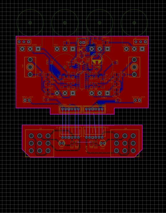
So I want to connect those two PCBs with a V-Cut or Stamp-hole so I can order all of this in one go.
I contacted JLCPCB online support, they told me I had to Panelize and ONLY use STAMP-HOLE, because V-cut + SMT assembly isn't supported.
So I did the Panelization, and I got this instead:
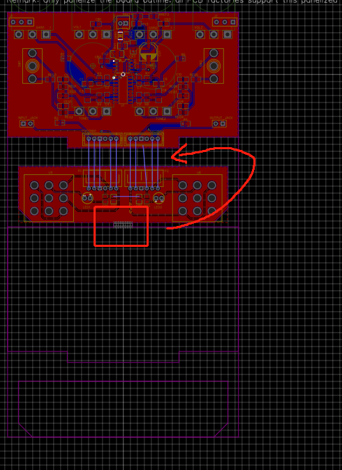
As you can see, the Stamp-hole is in the wrong position, It should connect both PCBs at the point I marked. I can't move (or dont know how) the stamp-hole to go between PCBs.
What am I doing wrong?
Please help.
Thank you!
Chrome
96.0.4664.93
Windows
10
EasyEDA
6.4.25

