
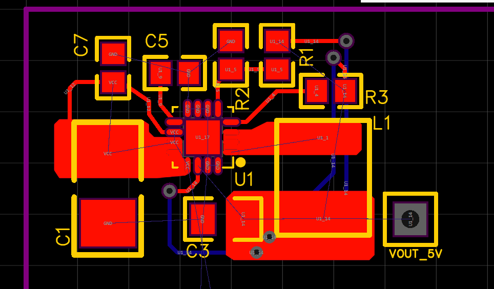
So here I'm using a solid region as according to the reccomended PCB layout for the IC that I'm using (data sheet link below). I want to make sure before I have the board made, the solid region will 1) Be connected to the pads its under (I made it have the same net) and 2) that only the actual solder pad of the components will be exposed on the board, if the whole solid region were exposed it would be difficult. If these things are not as intended, how would I change them so they would be?
Current layout:
Intended layout:

Datasheet:
[http://www.ti.com/lit/ds/symlink/tlv62130a.pdf](http://www.ti.com/lit/ds/symlink/tlv62130a.pdf)
Thanks


 Brand new interactions and interfaces.


 Easy to use and quick to get started.