

Good morning!
I was hoping I could get some advice for creating a proper PCB footprint that includes vias.
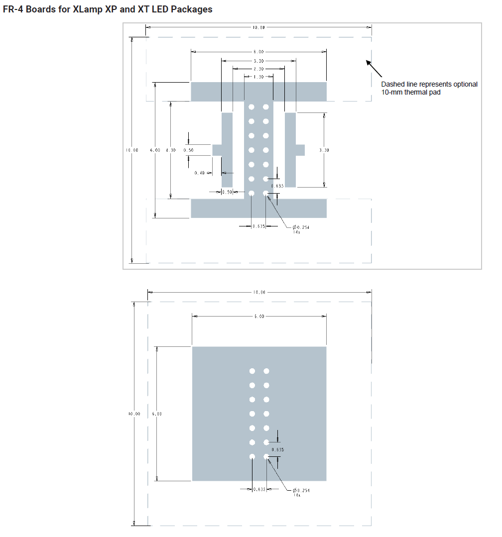
Here is the design information from Cree . . .
I have searched the Cree site for a GERBER file of the footprint to no avail.
The challenge I am having is I cannot create the "I\-Shape" footprint \*and\* place the vias through it without the DRC throwing errors\.
Here is a link to the PCB file I am attempting to implement the footprint in:
[LINK](https://easyeda.com/editor#id=%7C4522143fe79e4ad9b5561f8c0eb09bdd%7Ce978d9ec63cb482884e35731aa788c36%7C633c5693d6e64d0db00ed37d175288cf)
LED D01A shows the footprint I am trying to use. The others are using a workaround that is inadequate. I would like the "I-shape" footprint to be part of the THERMAL net so I can connect it to the grid filled THERMAL areas. If what I am trying to achieve is the wrong goal, please suggest what I should be doing instead.
Here is a dropbox link to the .json file of the footprint: [FOOTPRINT](https://www.dropbox.com/s/efjn96hx3lxxa9u/CREE%20XLAMP%20XP-E2%20TORCH%20LED%20NO%20VIA%20V2A.json?dl=0)
Here is the json text for the PCB footprint file in case that link does not work:
```
{
"head": {
"docType": "4",
"editorVersion": "6.2.38",
"c_para": {
"package": "CREE XLAMP XP-E2 TORCH LED NO VIA V2A",
"pre": "LED?",
"Contributor": "Darryl Lawler",
"link": ""
},
"hasIdFlag": true,
"x": 4000,
"y": 3000,
"uuid": "1b9dacb9886f499b933b071c0e08303e",
"utime": 1565266428,
"importFlag": 0,
"transformList": ""
},
"canvas": "CA~1000~1000~#000000~yes~#FFFFFF~0.393701~1000~1000~line~0.098425~mm~0.6299~45~visible~0.019685~4000~3000~0~yes",
"shape": [
"SOLIDREGION~2~~M 3988.189 2988.189 L 4011.811 2988.189 L 4011.811 3011.811 L3988.189,3011.811 Z~solid~gge150~~~~0",
"SOLIDREGION~1~~M 3988.189 2988.189 L 3988.189 2991.5354 L 3997.4409 2991.5354 L 3997.4409 3008.4646 L 3988.189 3008.4646 L 3988.189 3011.811 L 4011.811 3011.811 L 4011.811 3008.4646 L 4002.5591 3008.4646 L 4002.5591 2991.5354 L 4011.811 2991.5354 L 4011.811 2988.189 Z ~solid~gge303~~~~0",
"PAD~POLYGON~3994.488~3000~3.543~12.992~1~~ANODE~0~3993.5041 2993.5039 3995.4726 2993.5039 3995.4726 3006.4961 3993.5041 3006.4961 3993.5039 3000.9843 3991.9291 3000.9843 3991.9291 2999.0157 3993.5039 2999.0157~0~gge10~0~~Y~0~0~0.4~3994.4882,3000",
"PAD~POLYGON~4005.512~3000~3.543~12.992~1~~CATHODE~0~4004.5274 2993.5039 4006.496 2993.5039 4006.4961 2999.0157 4008.0709 2999.0157 4008.0709 3000.9843 4006.4961 3000.9843 4006.496 3006.4961 4004.5274 3006.4961~0~gge25~0~~Y~0~0~0.4~4005.5118,3000",
"TRACK~0.6299~3~S$31~3993 2993 4007 2993~gge30~0",
"TRACK~0.6299~3~S$31~3993 3007 4007 3007~gge32~0",
"TRACK~0.6299~3~S$31~3993 3007 3993 2993~gge33~0",
"TRACK~0.6299~3~S$31~4007 3007 4007 2993~gge34~0",
"TRACK~0.6299~3~S$31~4008 3007 4008 2993~gge35~0",
"PAD~ELLIPSE~3998.748~2992.5~1.3937~1.3937~11~~THPD1~0.5~~0~gge306~0~~Y~0~0~0.4~3998.7476,2992.4999",
"PAD~ELLIPSE~4001.252~2992.5~1.3937~1.3937~11~~THPD1~0.5~~0~gge316~0~~Y~0~0~0.4~4001.2517,2992.4999",
"PAD~ELLIPSE~4001.252~2995~1.3937~1.3937~11~~THPD1~0.5~~0~gge321~0~~Y~0~0~0.4~4001.2518,2994.9994",
"PAD~ELLIPSE~3998.748~2995~1.3937~1.3937~11~~THPD1~0.5~~0~gge326~0~~Y~0~0~0.4~3998.7476,2995.0004",
"PAD~ELLIPSE~4001.252~2997.5~1.3937~1.3937~11~~THPD1~0.5~~0~gge331~0~~Y~0~0~0.4~4001.2518,2997.4994",
"PAD~ELLIPSE~3998.748~2997.5~1.3937~1.3937~11~~THPD1~0.5~~0~gge336~0~~Y~0~0~0.4~3998.7477,2997.5004",
"PAD~ELLIPSE~4001.252~3000~1.3937~1.3937~11~~THPD1~0.5~~0~gge341~0~~Y~0~0~0.4~4001.2518,2999.9998",
"PAD~ELLIPSE~3998.748~3000~1.3937~1.3937~11~~THPD1~0.5~~0~gge346~0~~Y~0~0~0.4~3998.7477,2999.9998",
"PAD~ELLIPSE~4001.252~3002.558~1.3937~1.3937~11~~THPD1~0.5~~0~gge351~0~~Y~0~0~0.4~4001.2518,3002.5583",
"PAD~ELLIPSE~3998.748~3002.558~1.3937~1.3937~11~~THPD1~0.5~~0~gge356~0~~Y~0~0~0.4~3998.7477,3002.5583",
"PAD~ELLIPSE~4001.252~3005~1.3937~1.3937~11~~THPD1~0.5~~0~gge361~0~~Y~0~0~0.4~4001.2518,3004.9998",
"PAD~ELLIPSE~3998.748~3005~1.3937~1.3937~11~~THPD1~0.5~~0~gge366~0~~Y~0~0~0.4~3998.7477,3004.9998",
"PAD~ELLIPSE~4001.252~3007.5~1.3937~1.3937~11~~THPD1~0.5~~0~gge371~0~~Y~0~0~0.4~4001.2511,3007.4997",
"PAD~ELLIPSE~3998.748~3007.5~1.3937~1.3937~11~~THPD1~0.5~~0~gge376~0~~Y~0~0~0.4~3998.748,3007.4996"
],
"systemColor": "#000000~#FFFFFF~#FFFFFF~#222222~#FAD609",
"layers": [
"1~TopLayer~#FF0000~true~true~true~",
"2~BottomLayer~#0000FF~true~false~true~",
"3~TopSilkLayer~#FFCC00~true~false~true~",
"4~BottomSilkLayer~#66CC33~true~false~true~",
"5~TopPasteMaskLayer~#808080~true~false~true~",
"6~BottomPasteMaskLayer~#800000~true~false~true~",
"7~TopSolderMaskLayer~#800080~true~false~true~",
"8~BottomSolderMaskLayer~#AA00FF~true~false~true~",
"9~Ratlines~#6464FF~true~false~true~",
"10~BoardOutline~#FF00FF~true~false~true~",
"11~Multi-Layer~#C0C0C0~true~false~true~",
"12~Document~#FFFFFF~false~false~true~",
"13~TopAssembly~#33CC99~false~false~false~",
"14~BottomAssembly~#5555FF~false~false~false~",
"15~Mechanical~#F022F0~false~false~false~",
"21~Inner1~#800000~false~false~false~~",
"22~Inner2~#008000~false~false~false~~",
"23~Inner3~#00FF00~false~false~false~~",
"24~Inner4~#BC8E00~false~false~false~~",
"25~Inner5~#70DBFA~false~false~false~~",
"26~Inner6~#00CC66~false~false~false~~",
"27~Inner7~#9966FF~false~false~false~~",
"28~Inner8~#800080~false~false~false~~",
"29~Inner9~#008080~false~false~false~~",
"30~Inner10~#15935F~false~false~false~~",
"31~Inner11~#000080~false~false~false~~",
"32~Inner12~#00B400~false~false~false~~",
"33~Inner13~#2E4756~false~false~false~~",
"34~Inner14~#99842F~false~false~false~~",
"35~Inner15~#FFFFAA~false~false~false~~",
"36~Inner16~#99842F~false~false~false~~",
"37~Inner17~#2E4756~false~false~false~~",
"38~Inner18~#3535FF~false~false~false~~",
"39~Inner19~#8000BC~false~false~false~~",
"40~Inner20~#43AE5F~false~false~false~~",
"41~Inner21~#C3ECCE~false~false~false~~",
"42~Inner22~#728978~false~false~false~~",
"43~Inner23~#39503F~false~false~false~~",
"44~Inner24~#0C715D~false~false~false~~",
"45~Inner25~#5A8A80~false~false~false~~",
"46~Inner26~#2B937E~false~false~false~~",
"47~Inner27~#23999D~false~false~false~~",
"48~Inner28~#45B4E3~false~false~false~~",
"49~Inner29~#215DA1~false~false~false~~",
"50~Inner30~#4564D7~false~false~false~~",
"51~Inner31~#6969E9~false~false~false~~",
"52~Inner32~#9069E9~false~false~false~~"
],
"objects": [
"All~true~false",
"Component~true~true",
"Prefix~true~true",
"Name~true~false",
"Track~true~true",
"Pad~true~true",
"Via~true~true",
"Hole~true~true",
"Copper_Area~true~true",
"Circle~true~true",
"Arc~true~true",
"Solid_Region~true~true",
"Text~true~true",
"Image~true~true",
"Rect~true~true",
"Dimension~true~true",
"Protractor~true~true"
],
"BBox": {
"x": 3988.2,
"y": 2988.2,
"width": 23.6,
"height": 23.6
},
"netColors": {}
}
```
One challenge I am having is properly masking the footprint so the anode, cathode and thermal pad areas are exposed, but the top and bottom of the "I-shape" footprint is solder masked. Additionally, the pad + vias combination is throwing a DRC error for each via. If I could set the net for the "I-shape" footprint to THERMAL or TPD1, I believe it would work, but I don't know how to set the net for an "area" in the footprint editor.


 Brand new interactions and interfaces.


 Easy to use and quick to get started.