You need to use EasyEDA editor to create some projects before publishing
Yellow cross on pad component
2153 19
martin.denion 3 years ago
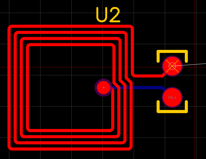
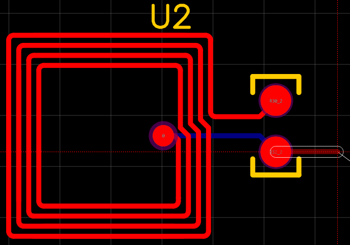
I am currently adding an NFC antenna to my board. However, I cannot connect one of the pads of my antenna to the corresponding component. Indeed, when I want to connect the top pad of this antenna, a yellow cross appears, while it works for the bottom pad. However, I have associated the antenna schematic to the footprint. Can you help me ? Click [here](https://easyeda.com/component/5ebdd721e2a3421f97ebfb3d06dd969f) to see my component: ![image.png](//image.easyeda.com/pullimage/NDqOR5Y57GKjqRr5R71DtpqlY8DlL7nDLZuwWsQT.png) ![image.png](//image.easyeda.com/pullimage/XCxHg2j8KOcAaYhQg42dCEoPS2G7jKDTLQDzZEPt.png) 
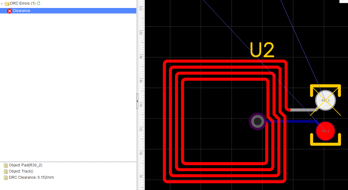
Here is the DRC error I get: ![image.png](//image.easyeda.com/pullimage/pRY8WMJlBBGshksFhZirYZvlfhmRGUDH60isfXIp.png)
Comments
andyfierman 3 years ago
This subject keeps coming up... Please see my comments - and follow the links in - my comments in: [https://easyeda.com/forum/topic/Non-exposed-coper-vias-in-footprints-341192f38fb04a1b8addae2065ba400c](https://easyeda.com/forum/topic/Non-exposed-coper-vias-in-footprints-341192f38fb04a1b8addae2065ba400c)
Reply
andyfierman 3 years ago
Also: [https://easyeda.com/forum/topic/Net-tie-a-copper-only-component-with-2-pads-to-split-nets-without-DRC-errors-and-multiple-netname-warnings-b6a099bf01bb4055b821ab398ee37b60](https://easyeda.com/forum/topic/Net-tie-a-copper-only-component-with-2-pads-to-split-nets-without-DRC-errors-and-multiple-netname-warnings-b6a099bf01bb4055b821ab398ee37b60)
Reply
martin.denion 3 years ago
Thank you for your comments. I have read almost all your comments/tips and I have one question before going any further: is it possible to design an NFC coil antenna on EasyEDA?
Reply
martin.denion 3 years ago
@andyfierman Please check my edited post so you can help me solving the clearance error :)
Reply
andyfierman 3 years ago
"...is it possible to design an NFC coil antenna on EasyEDA?" Yes and no. You can not use EasyEDA to "design" a PCB antenna. It is not an antenna design tool. That requires a very different and specialist RF and Microwave EDA tool. It is, however,  possible to create the footprint for any PCB antenna but, subject to the outcome of my recent Feature Request: [https://easyeda.com/forum/topic/Net-tie-a-copper-only-component-with-2-pads-to-split-nets-without-DRC-errors-and-multiple-netname-warnings-b6a099bf01bb4055b821ab398ee37b60](https://easyeda.com/forum/topic/Net-tie-a-copper-only-component-with-2-pads-to-split-nets-without-DRC-errors-and-multiple-netname-warnings-b6a099bf01bb4055b821ab398ee37b60)<br> <br> at the moment you have to read, understand and follow the rules set out in the text and links below: EasyEDA has no concept of a netname-splitting short-circuit element so PCB antennas in EasyEDA are horrible to deal with but this particular footprint is a nightmare: it will generate many DRC errors anyway because the spiral is constructed on track not pads and there are two pads each with different numbers plus one with no number whereas if the whole thing is made of pads and they are all given the same number then the footprint is at least consistent with this topic: [https://easyeda.com/forum/topic/How-to-avoid-DRC-errors-when-connecting-to-PCB-Footprints-a-k-a-PCB-Libs-90bf944fe3644b21a7d27a9e9d8df8d6](https://easyeda.com/forum/topic/How-to-avoid-DRC-errors-when-connecting-to-PCB-Footprints-a-k-a-PCB-Libs-90bf944fe3644b21a7d27a9e9d8df8d6) and you only have to deal with making the antenna connections so that they have the same netnames. If you have an antenna matching (RF) pad or network then that is not usually a problem although it might look a little odd in the schematic as the antenna port of the matching network will probably have to be named ground. See also: [https://easyeda.com/forum/topic/How-to-design-a-PCB-Lib-for-a-PCB-Antenna-efa50ba1cdd9433c958ceedbad520398](https://easyeda.com/forum/topic/How-to-design-a-PCB-Lib-for-a-PCB-Antenna-efa50ba1cdd9433c958ceedbad520398) [https://easyeda.com/forum/topic/Weird-Pad-Behavior-Traces-Not-Connecting-Properly-4660a264d69843b99ed5d5c735da4a96](https://easyeda.com/forum/topic/Weird-Pad-Behavior-Traces-Not-Connecting-Properly-4660a264d69843b99ed5d5c735da4a96) [https://easyeda.com/forum/topic/Cannot-get-antennas-pad-to-connect-to-any-track-2019598319464657b86a6bc0837d97a3](https://easyeda.com/forum/topic/Cannot-get-antennas-pad-to-connect-to-any-track-2019598319464657b86a6bc0837d97a3)<br> <br> The takeaway from this is that if you do not include a 0R resistor or a matching network in series with your PCB antenna you have to accept that either the antenna ("hot") port in your schematic must have the same netlabel as the "cold" or ground end of you antenna or you must temporarily set **Routing Conflict > Ignore** to connect to the hot port to the hot end of the antenna and put up with the DRC errors that will generate.
Reply
martin.denion 3 years ago
@andyfierman Can you specify where exactly this zero ohm resistor should be added?
Reply
andyfierman 3 years ago
Taking an NFC antenna as an example and assuming you have built the antenna as described in: [https://easyeda.com/forum/topic/How-to-avoid-DRC-errors-when-connecting-to-PCB-Footprints-a-k-a-PCB-Libs-90bf944fe3644b21a7d27a9e9d8df8d6](https://easyeda.com/forum/topic/How-to-avoid-DRC-errors-when-connecting-to-PCB-Footprints-a-k-a-PCB-Libs-90bf944fe3644b21a7d27a9e9d8df8d6)<br> <br> so it consists of nothing but pads all having the same number then you have 2 pads both having the same number (for example "1") connected by a spiral track also made of one or more pads with the same number ("1"): then you connect the pad at one end of the spiral to ground (call this the cold end) and the pad at the other end of the spiral (call this the hot end) goes to the antenna pin on some device. You route a length of track from the hot end to one end of a 0R resistor then route a length of track from the other end of the resistor to the antenna pin on the device.
Reply
martin.denion 3 years ago
@andyfierman Ok, so do I have to convert to Pad each piece of my spiral track or can I leave it like that? Then, in what file exactly should I add this 0R resistor? In the shematic file and then route it in the PCB file as you said? Because I don't understand why adding a 0R resistance will remove this DRC error. PCB antenna symbol: ![image.png](//image.easyeda.com/pullimage/U1WHqfuBRPty21NJ7wb8mCPaDyP52aI0YTr017dh.png) PCB antenna footprint: ![image.png](//image.easyeda.com/pullimage/7yn9lBM3vmlOdtG3f4PAbngnWcgP9WHCD1iXVgoQ.png) PCB antenna in my PCB file: ![image.png](//image.easyeda.com/pullimage/e0E3nHbk3rhABHxbHshGx4piRYBmMUoxcMGkMpPY.png)
Reply
andyfierman 3 years ago
"do I have to convert to Pad each piece of my spiral track" Yes. "...should I add this 0R resistor? In the shematic file and then route it in the PCB file as you said?" Yes.
Reply
martin.denion 3 years ago
Ok so I don't have the DRC error anymore since I converted each piece of my spiral into a Pad and renumbered them all to "1", which is already a very good point, thank you! Again, sorry for my misunderstanding but I added a 0R resistor as you said but I don't see the point of adding it because the two antenna ports still want to be routed together. ![image.png](//image.easyeda.com/pullimage/FCHFYDhOXZ7aWgu55Duor2NZ3TQwonRvaH5QMrGo.png) ![image.png](//image.easyeda.com/pullimage/ie9ippZOpauDqX5K0Rznzax0KLfapwO3o9zd4pdy.png)
Reply
andyfierman 3 years ago
"... I don't understand why adding a 0R resistance will remove this DRC error." A PCB antenna is a piece of copper. It's  a short circuit. Therefore it cannot have two different net names. Therefore whatever nets connect to each end of it has to be assigned the same net name. If one end connects to GND then the other end has to be labelled as GND too which looks odd when that end is the transceiver i/o pin on a chip. Adding the 0R allows the chip i/o pin to have a sensible name and both nets in the antenna to be the same and have no DRC errors. You do have to think very carefully about how any copper areas with the same net name as the antenna are then laid out to avoid just flooding the antenna. In fact if you put the 0R link in the "cold" end instead of the "hot" end then that problem goes away too. <br> <br>
Reply
martin.denion 3 years ago
Okay, thank you for your explanation. So, for you, in the end, is it normal that both antenna ports always want to be routed together? And is the renaming of the antenna pads suitable for you?
Reply
andyfierman 3 years ago
@martin.denion, I don't really understand your questions: "...is it normal that both antenna ports always want to be routed together? And is the renaming of the antenna pads suitable for you?" Any PCB antenna or inductor is just a piece of copper so it cannot have a different net name connected to it at each end. It also cannot have a different pad number at each end unless you are prepared to accept that the footprint will geberate a DRC error. There is no question of naming pads. They do not have a Name attribute only a Number attribute.
Reply
martin.denion 3 years ago
@andyfierman I meant that there is a blue link between the two ports of the antenna which means that I have to route the two ports together, how do I make it not appear anymore? Then, for the second question, I meant "renumbering", not "renaming".
Reply
andreasbernhofer 3 years ago
Okay, so it is clear that footprints like this NFC coil etc. cannot be made without workarounds or accepting errors. However, can someone explain to me why it seems to be most important for all to not have DRC errors? Creating the footprint without DRC errors requires other sacrifices like using only one pad number for both pads, using pads for tracks and vias and also adding a dummy-resistor or something similar to the schematic. You also have to accept that this may allow you to accidentally connect a track to the track of the coil instead of the pad and this won't throw an error either. Why not create the footprint as regular, with two pads, tracks and vias, and accept that it will show two DRC errors on the pads? It's a known limitation, but way less of a workaround... Isn't this a valid option? 🤔
Reply
andyfierman 3 years ago
@andreasbernhofer, I don't think I said that wasn't a valid option: "It also cannot have a different pad number at each end unless you are prepared to accept that the footprint will generate a DRC error." Footprints can be made anyhow you like with pads of any numeration and with tracks and solid regions. All you have to do is decide if you are happy to remember what each of the DRC errors - which will be generated by not making everything out of pads and by not.giving all pads that are connected together by copper within the Footprint the same pad number - refer to every time you run the PCB Design Manager. Until the underlying problems with how Design Rules are applied to and reported for Footprints and maybe a "net-tie" element is introduced, then the choices of keeping track of multiple DRC errors and using some simple rules to design Footprints to minimise the generation of DRC errors will remain. All I have described is an entirely optional alternative way to work round those DRC errors.
Reply
andyfierman 3 years ago
Sorry, missed a phrase out... "Until the underlying problems with how Design Rules are applied to and reported for Footprints **are corrected**..."
Reply
andreasbernhofer 3 years ago
Okay thx ;) I just wasn't sure if there may be a strong / technical reason for not having DRC errors. So as there is not, I guess my preferred solution would be to live with these errors, but I fully understand that this is not the preferred solution for everyone. Just wanted to make clear that this is also a valid option. I've read your thread on the net tie, that's also an interesting concept. I guess an alternative could be how the DRC net rules are checked. I think basically it would be enough if DRC net rules are checked against a PAD of a footprint, that the DRC rule checker assumes that all tracks of the footprint that are touching this pad are part of the same net, regardless of their assigned net, just for the moment of checking. So when PAD1 is checked, the track connecting PAD1 and PAD2 is assumed to be the same net as PAD1. And when PAD2 is checked, the track is assumed to be the same net as PAD2. And when the track itself is checked against any other thing that is not part of the footprint, it is just a random net that's not used anywhere else...
Reply
andyfierman 3 years ago
@andreasbernhofer, Yes, I think maybe it's time to raise a feature request that: 1. tabulates some basic design rules for footprints and;  2. how those rule are checked within the footprint as it is being created and then;  3. how the PCB DRC is applied to the Footprint once it has been placed in a PCB. As far as footprints for PCB antennas and inductors (spiral tracks) are concerned if the design rules are made to allow for pads being connected to each other by copper within the footprint (i.e. a DRC error can be permanently disabled once it has been generated as a warning to the constructor) then there  is no longer a need for a component or a net-tie in series with them because copper connected footprints can have different pad numbers even though they are shorted by copper within the footprint. There is still a usage case for a net-tie where it is helpful to retain separate net names from within a schematic once it has been passed into PCB. That would simplify for example the ground flooding around things like Kelvin connections to current sense resistors and 4th pin Source connections to SiC and GAN FETs.
Reply
Login or Register to add a comment
goToTop
你现在访问的是EasyEDA海外版,建议访问速度更快的国内版 https://lceda.cn(需要重新注册)
如果需要转移工程请在个人中心 - 工程 - 工程高级设置 - 下载工程,下载后在https://lceda.cn/editor 打开保存即可。
有问题联系QQ 3001956291 不再提醒
svg-battery svg-battery-wifi svg-books svg-more svg-paste svg-pencil svg-plant svg-ruler svg-share svg-user svg-logo-cn svg-double-arrow -mockplus- -mockplus- -mockplus- -mockplus- -mockplus- -mockplus- -mockplus- -mockplus-@1x -mockplus-

Cookie Notice

Our website uses essential cookies to help us ensure that it is working as expected, and uses optional analytics cookies to offer you a better browsing experience. To find out more, read our Cookie Notice